RX62Nグループ、RX621グループ
5. Electrical Characteristics
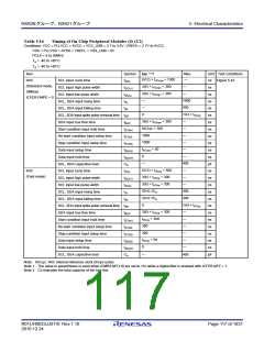
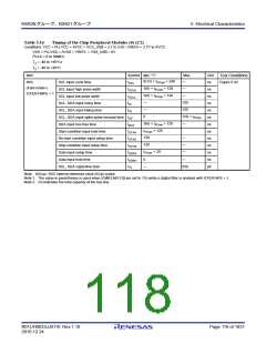
Table 5.16
Timing of On-Chip Peripheral Modules (4) (2/2)
Conditions: VCC = PLLVCC = AVCC = VCC_USB = 2.7 to 3.6V, VREFH = 2.7V to AVCC
VSS = PLLVSS = AVSS = VREFL = VSS_USB = 0V
PCLK = 8 to 50MHz
Ta = -40 to +85Cz
Ta = -40 to +85C
Min.*1*2
Item
Symbol
tSCL
tSCLH
tSCLL
tSr
Max.
Unit
Test Conditions
6(12) × tIICcyc + 240
—
RIIC
SCL input cycle time
ns
ns
ns
ns
ns
ns
ns
ns
ns
ns
ns
ns
pF
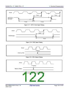
Figure 5.43
(Fast-mode+)
ICFER.FMPE = 1
3(6) × tIICcyc + 120
—
SCL input high pulse width
SCL input low pulse width
SCL, SDA input rising time
SCL, SDA input falling time
3(6) × tIICcyc + 120
—
—
120
—
120
tSf
0
1(4) × tIICcyc
—
SCL, SDA input spike pulse removal time tSP
3(6) × tIICcyc + 120
tIICcyc + 120
120
SDA input bus free time
tBUF
Start condition input hold time
Re-start condition input setup time
Stop condition input setup time
Data input setup time
tSTAH
tSTAS
tSTOS
tSDAS
tSDAH
Cb
—
—
—
120
tIICcyc + 20
Data input hold time
0
—
SCL, SDA capacitive load
—
550
Note: tIICcyc: RIIC internal reference clock (IICφ) cycles
Note 1. The value in parentheses is used when ICMR3.NF[1:0] are set to 11b while a digital filter is enabled with ICFER.NFE = 1.
Note 2. Cb indicates the total capacity of the bus line.
R01UH0033JJ0110 Rev.1.10
2010.12.24
Page 118 of 1931

 RENESAS [ RENESAS TECHNOLOGY CORP ]