RX62Nグループ、RX621グループ
5. Electrical Characteristics
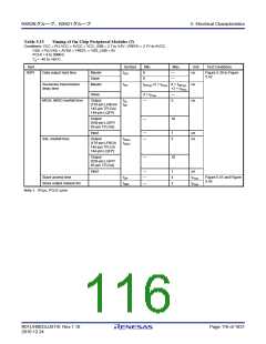
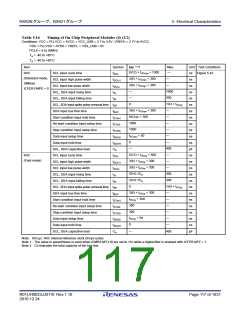
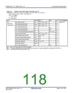
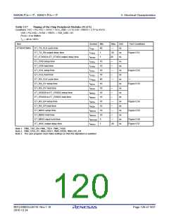
Table 5.17
Timing of On-Chip Peripheral Modules (5) (2/2)
Conditions: VCC = PLLVCC = AVCC = VCC_USB = 2.7 to 3.6V, VREFH = 2.7V to AVCC
VSS = PLLVSS = AVSS = VREFL = VSS_USB = 0V
PCLK = 8 to 50MHz
Ta = -40 to +85C
Item
Symbol Min.
Max. Unit
Test Conditions
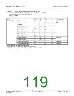
ETHERC(MII)
ET_TX_CLK cycle time
ET_TX_EN output delay time
ET_ETXD0 to ET_ETXD3 output delay time
ET_CRS setup time
tTcyc
40
1
—
ns
ns
ns
ns
ns
ns
ns
ns
ns
ns
ns
ns
ns
ns
ns
ns
ns
ns
—
tTENd
tMTDd
tCRSs
tCRSh
tCOLs
tCOLh
tTRcyc
tRDVs
tRDVh
tMRDs
tMRDh
tRERs
tRESh
tMDIOs
tMDIOh
tMDIOdh
tWOLd
20
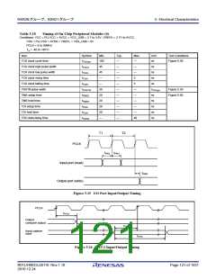
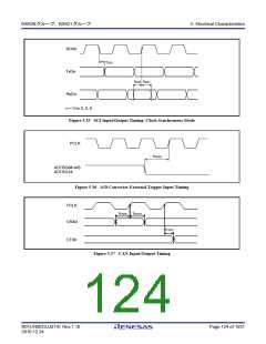
Figure 5.51
1
20
10
10
10
10
40
10
10
10
10
10
10
10
10
5
—
—
ET_CRS hold time
ET_COL setup time
—
Figure 5.52
ET_COL hold time
—
ET_RX_CLK cycle time
ET_RX_DV setup time
—
—
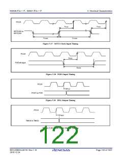
Figure 5.53
ET_RX_DV hold time
—
—
—
ET_ERXD0 to ET_ERXD3 setup time
ET_ERXD0 to ET_ERXD3 hold time
ET_RX_ER setup time
—
Figure 5.54
Figure 5.55
ET_RX_ER hold time
—
ET_MDIO setup time
—
ET_MDIO hold time
—
ET_MDIO utput hold time
ET_WOL output delay time
—
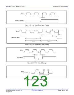
Figure 5.56
Figure 5.57
1
20
Note 1. RMII_TXD_EN, RMII_TXD1, RMII_TXD0
Note 2. RMII_CRS_DV, RMII_RXD1, RMII_RXD0, RMII_RX_ER
Note 3. The user program must make settings so that this stipulation is satisfied.
R01UH0033JJ0110 Rev.1.10
2010.12.24
Page 120 of 1931

 RENESAS [ RENESAS TECHNOLOGY CORP ]