RX62Nグループ、RX621グループ
5. Electrical Characteristics
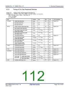
Table 5.14
Timing of On-Chip Peripheral Modules (2) (1/2)
Conditions: VCC = PLLVCC = AVCC = VCC_USB = 2.7 to 3.6V, VREFH = 2.7V to AVCC
VSS = PLLVSS = AVSS = VREFL = VSS_USB = 0V
PCLK = 8 to 50MHz
Ta = -40 to +85C
Item
CAN
Symbol
tCTXD
Min.
—
Max.
40.0
Unit
ns
Test Conditions
Figure 5.37
Transmit data delay time
Receive data setup time
Receive data hold time
tCRXS
tCRXH
tSPcyc
40.0
40.0
2
—
ns
—
ns
*1
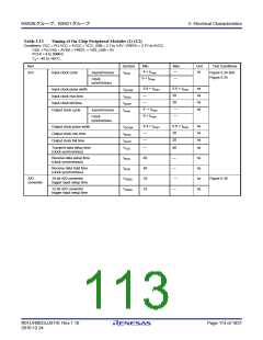
RSPI
RSPCK clock cycle
Master
4096
4096
Figure 5.38
tPcyc
Slave
8
RSPCK clock
high pulse width
Master
tSPCKWH
(tSPcyc-tSPCKR-tSPCKF
2-3
)
/
—
ns
ns
ns
Slave
(tSPcyc-tSPCKR-tSPCKF) / 2
—
RSPCK clock
low pulse width
Master
tSPCKWL
(tSPcyc-tSPCKR-tSPCKF
2-3
)
/
—
Slave
(tSPcyc-tSPCKR-tSPCKF) / 2
—
—
RSPCK clock
rise/fall time
Output
tSPCKr,
tSPCKf
5
[176-pin LFBGA/
145-pin TFLGA/
144-pin LQFP]
Output
[100-pin LQFP/
85-pin TFLGA]
—
—
10
1
Input
µs
Note 1. tPcyc: PCLK cycle
R01UH0033JJ0110 Rev.1.10
2010.12.24
Page 114 of 1931

 RENESAS [ RENESAS TECHNOLOGY CORP ]