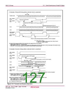
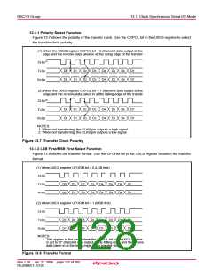
R8C/13 Group
13.2 Clock Asynchronous Serial I/O (UART) Mode
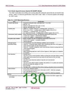
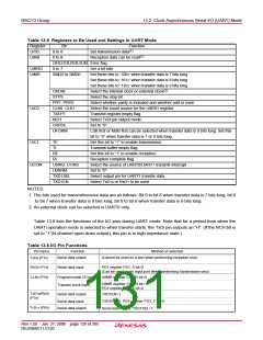
Table 13.5 Registers to Be Used and Settings in UART Mode
Register
UiTB
Bit
0 to 8
0 to 8
OER,FER,PER,SUM Error flag
Function
Set transmission data(1)
Reception data can be read(1)
UiRB
UiBRG
UiMR
0 to 7
Set a bit rate
SMD2 to SMD0
Set these bits to ‘1002’ when transfer data is 7 bits long
Set these bits to ‘1012’ when transfer data is 8 bits long
Set these bits to ‘1102’ when transfer data is 9 bits long
Select the internal clock or external clock(2)
Select the stop bit
CKDIR
STPS
PRY, PRYE
CLK0, CLK1
TXEPT
Select whether parity is included and whether odd or even
Select the count source for the UiBRG register
Transmit register empty flag
UiC0
NCH
Select TxDi pin output mode
CKPOL
UFORM
Set to “0”
LSB first or MSB first can be selected when transfer data is 8 bits long. Set this
bit to “0” when transfer data is 7 or 9 bits long.
Set this bit to “1” to enable transmission
Transmit buffer empty flag
UiC1
TE
TI
RE
Set this bit to “1” to enable reception
Reception complete flag
RI
UCON
U0IRS, U1IRS
U0RRM
TXD1SEL
TXD1EN
Select the source of UART0/UART1 transmit interrupt
Set to “0”
Select output pin for UART1 transfer data
Select TxD10 or RxD1 to be used
NOTES:
1. The bits used for transmit/receive data are as follows: Bit 0 to bit 6 when transfer data is 7 bits long; bit 0
to bit 7 when transfer data is 8 bits long; bit 0 to bit 8 when transfer data is 9 bits long.
2. An external clock can be selected in UART0 only.
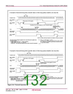
Table 13.6 lists the functions of the I/O pins during UART mode. Note that for a period from when the
UARTi operation mode is selected to when transfer starts, the TxDi pin outputs an “H”. (If the NCH bit is
set to “1”(N-channel open-drain output), this pin is in high-impedance state.)
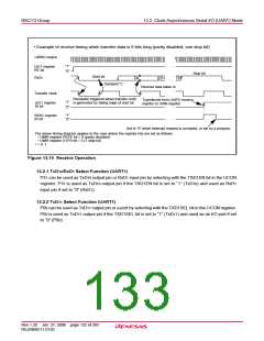
Table 13.6 I/O Pin Functions
Pin name
Function
Method of selection
TxD (P1
0
4)
Serial data output
(Cannot be used as a port when performing reception only)
RxD
0
0
(P1
5
)
Serial data input
PD1 register PD1_5 bit=0
(Can be used as an input port when performing transmission only)
CLK
(P16
)
Programmable I/O port
Transfer clock input
U0MR register CKDIR bit=0
U0MR register CKDIR bit=1
PD1 register PD1_6 bit=0
TxD10/RxD
1
Serial data output
TXD1EN=1
(P3
7
)
TXD1EN=0, PD3 register PD3_7 bit=0
Serial data output, TXD1SEL=1
Serial data input
Serial data output
TxD11 (P00)
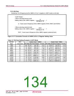
Rev.1.20 Jan 27, 2006 page 120 of 205
REJ09B0111-0120

 RENESAS [ RENESAS TECHNOLOGY CORP ]