R8C/13 Group
13.2 Clock Asynchronous Serial I/O (UART) Mode
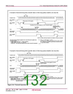
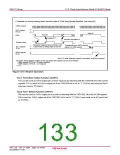
• Example of receive timing when transfer data is 8 bits long (parity disabled, one stop bit)
UiBRG output
“1”
“0”
UiC1 register
RE bit
Stop bit
Start bit
Sampled “L”
RxDi
D0
D
1
D7
Receive data taken in
Transfer clock
Reception triggered when transfer clock
is generated by falling edge of start bit
Transferred from UARTi receive
register to UiRB register
“1”
“0”
UiC1 register
RI bit
“1”
“0”
SiRIC register
IR bit
Set to “0” when interrupt request is accepted, or set by a program
The above timing diagram applies to the case where the register bits are set as follows:
• UiMR register PRYE bit = 0 (parity disabled)
• UiMR register STPS bit = 0 (1 stop bit)
i = 0, 1
Figure 13.10 Receive Operation
13.2.1 TxD10/RxD1 Select Function (UART1)
P37 can be used as TxD10 output pin or RxD1 input pin by selecting with the TXD1EN bit in the UCON
register. P37 is used as TxD10 output pin if the TXD1EN bit is set to “1” (TxD10) and used as RxD1
input pin if set to “0” (RxD1).
13.2.2 TxD11 Select Function (UART1)
P00 can be used as TxD11 output pin or a port by selecting with the TXD1SEL bit in the UCON register.
P00 is used as TxD11 output pin if the TXD1SEL bit is set to “1” (TxD11) and used as an I/O port if set
to “0” (P00).
Rev.1.20 Jan 27, 2006 page 122 of 205
REJ09B0111-0120

 RENESAS [ RENESAS TECHNOLOGY CORP ]