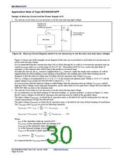
M51995AP/AFP
Current Limiting Circuit
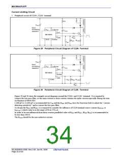
1. Peripheral circuit of CLM+, CLM− terminal
R1
+
CFIN
Input
smoothing
VCC
capacitor
+
Collector
VOUT
CVCC
M51995A
RNF1
CLM+
Emitter
GND
RCLM
RNF2
CNF
Figure 29 Peripheral Circuit Diagram of CLM+ Terminal
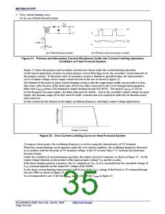
R1
+
CFIN
Input
smoothing
capacitor
+
VCC
Collector
VOUT
CVCC
M51995A
Emitter
GND
CNF RNF2 RCLM
CLM−
RNF1
Figure 30 Peripheral Circuit Diagram of CLM− Terminal
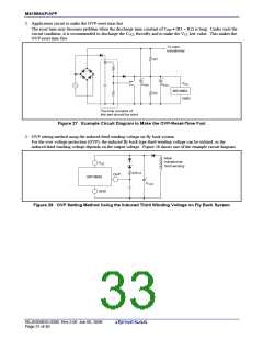
Figure 29 and 30 show the example circuit diagrams around the CLM+ and CLM− terminal. It is required to
connect the low pass filter, as the main current or drain current contains the spike current especially during the turn-
on duration of MOS FET.
1,000 pF to 22,000 pF is recommended for CNF and the RNF1 and RNF2 have the functions both to adjust the “current-
detecting-sensitivity” and to consist the low pass filter.
To design the RNF1 and RNF2, it is required to consider the influence of CLM terminal source current (IINCLM+ or
INFCLM−), which value is in the range of 90 to 270 µA.
In order to be not influenced from these resistor paralleled value of RNF1 and RNF2, (RNF1/RNF2) is recommended to
be less than 100 Ω.
The RCLM should be the non-inductive resistor.
REJ03D0835-0300 Rev.3.00 Jun 06, 2008
Page 32 of 40

 RENESAS [ RENESAS TECHNOLOGY CORP ]