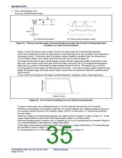
M51995AP/AFP
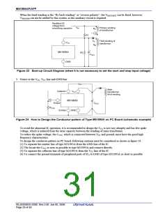
When the third winding is the “fly back winding” or “reverse polarity”, the VIN(START) can be fixed, however,
V
IN(STOP) can not be settled by this system, so the auxiliary circuit is required.
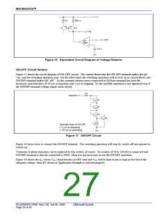
Rectified DC
voltage from
smoothing capacitor
VIN
Primary winding
of transformer
NP
R1
VF
NB
Third winding of
transformer
VCC
M51995A
GND
+
R2
CVCC
Figure 23 Start-up Circuit Diagram (when it is not necessary to set the start and stop input voltage)
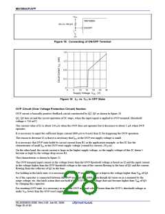
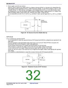
3. Notice to the VCC, VCC line and GND line
Main
transformer
third winding
Collector
VCC
+
M51995A
CVCC
Output
RCLM
Emitter
GND
Figure 24 How to Design the Conductor-pattern of Type M51995A on PC Board (schematic example)
To avoid the abnormal IC operation, it is recommended to design the VCC is not vary abruptly and has few spike
voltage, which is induced from the stray capacity between the winding of main transformer.
To reduce the spike voltage, the CVCC, which is connected between VCC and ground, must have the good high
frequency characteristics.
To design the conductor-pattern on PC board, following cautions must be considered as shown in figure 24.
(1) To separate the emitter line of type M51995A from the GND line of the IC
(2) The locate the CVCC as near as possible to type M51995A and connect directly
(3) To separate the collector line of type M51995A from the VCC line of the IC
(4) To connect the ground terminals of peripheral parts of ICS to GND of type M51995A as short as possible
REJ03D0835-0300 Rev.3.00 Jun 06, 2008
Page 29 of 40

 RENESAS [ RENESAS TECHNOLOGY CORP ]