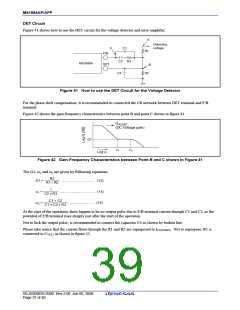
M51995AP/AFP
2. MOS FET gate drive power dissipation
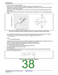
Figure 39 shows the relation between the applied gate voltage and the stored gate charge.
In the region 1, the charge is mainly stored at CGS as the depletion is spread and CGD is small owing to the off-state
of MOS FET and the high drain voltage.
In the region 2, the CGD is multiplied by the “mirror effect” as the characteristics of MOS FET transfers from off-
state to on-state.
In the region 3, both the CGD and CGS affect to the characteristics as the MOS FET is on-state and the drain voltage
is low.
20
Drain
ID
VDS = 80 V
200 V
320 V
15
10
5
CGD
(3)
Gate
VD
CDS
(2)
C
GS
VGS
(1)
ID = 4 A
Source
0
0
4
8
12
16
20
Total Stored Gate Charge (nC)
Figure 39 The Relation between Applied Gate-Source Voltage and Stored Gate Charge
The charging and discharging current caused by this gate charge makes the gate power dissipation. The relation
between gate drive current ID and total gate charge QGSH is shown by following equation;
ID = QGSH • fOSC ……………………………………………… (11)
Where
fosc is switching frequency
As the gate drive current may reach up to several tenths milliamperes at 500 kHz operation, depending on the size of
MOS FET, the power dissipation caused by the gate current can not be neglected.
In this case, following action will be considered to avoid heat up of type M51995A.
(1) To attach the heat sink to type M51995A
(2) To use the printed circuit board with the good thermal conductivity
(3) To use the buffer circuit shown next section
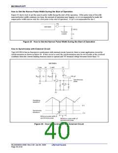
3. Output buffer circuit
It is recommended to use the output buffer circuit as shown in figure 40, when type M51995A drives the large
capacitive load or bipolar transistor.
VOUT
M51995A
Figure 40 Output Buffer Circuit Diagram
REJ03D0835-0300 Rev.3.00 Jun 06, 2008
Page 36 of 40

 RENESAS [ RENESAS TECHNOLOGY CORP ]