M51995AP/AFP
However, the M51995A will non-operate and operate intermittently, as the VCC voltage rises in accordance with
the decrease of ICC current.
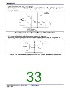
The fly back system has the constant output power characteristics as shown in figure 35 when the peak primary
current and the operating frequency are constant.
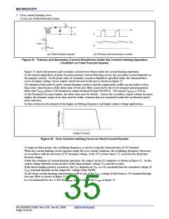
To control the increase of DC output current, the operating frequency is decreased using the characteristics of
VF terminal when the over current limiting function begins to operate.
The voltage which mode by dividing the VCC is applied to VF terminal as shown in figure 36, as the induced
third winding voltage depends on the DC output voltage of SMPS.
15 kΩ or less is recommended for R2 in figure 36, it is noticed that the current flows through R1 and R2 will
superpose on the ICC(START) current.
If the R1 is connected to CVCC2 in figure 25, the current flows through R1 and R2 is independent of the ICC(START)
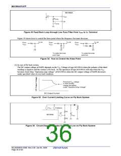
(3) Application circuit to keep the non-operating condition when over load current condition will continue for
specified duration
.
The CT terminal voltage will begin to rise and the capacitor connected to CT terminal will be charged-up, if the
current limiting function starts, and VF terminal voltage decreases below VTHTIME (∼ 3 V).
If the charged-up CT terminal voltage is applied to OVP terminal through the level-shifter consisted of buffer
transistor and resistor, it makes type M51995A keep non-operating condition.
VCC
CT
+
CT
M51995A
OVP
Figure 37 Application Circuit Diagram to Keep the Non-Operating Condition when Over Load Current
Condition will Continue for Specified Duration
Output Circuit
1. The output terminal characteristics at the VCC voltage lower than the “Operation-stop” voltage
The output terminal has the current sink ability even though the VCC voltage lower than the “Operation-stop”
voltage or VCC(STOP) (It means that the terminal is “Output low state” and please refer characteristics of output low
voltage versus sink current.)
This characteristics has the merit not to damage the MOS FET at the stop of operation when the VCC voltage
decreases lower than the voltage of VCC (STOP), as the gate charge of MOS FET, which shows the capacitive load
characteristics to the output terminal, is drawn out rapidly.
The output terminal has the draw-out ability above the VCC voltage of 2 V, however, lower than the 2 V, it loses the
ability and the output terminal potential may rise due to the leakage current.
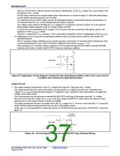
In this case, it is recommended to connect the resistor of 100 kΩ between gate and source of MOS FET as shown in
figure 38.
To main
transformer
VOUT
M51995A
100 kΩ
RCLM
Figure 38 Circuit Diagram to Prevent the MOS FET Gate Potential Rising
REJ03D0835-0300 Rev.3.00 Jun 06, 2008
Page 35 of 40

 RENESAS [ RENESAS TECHNOLOGY CORP ]