M51995AP/AFP
VCC
M51995A
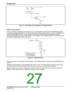
ON/OFF
30 k to 100 kΩ
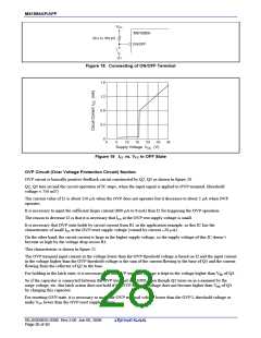
Figure 18 Connecting of ON/OFF Terminal
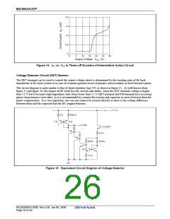
1.6
1.2
0.8
0.4
0
0
5
10
15
20
25
30
Supply Voltage VCC (V)
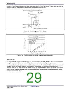
Figure 19 ICC vs. VCC in OFF State
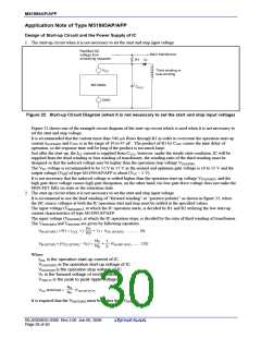
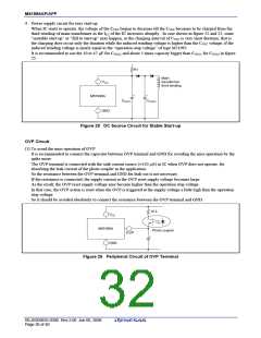
OVP Circuit (Over Voltage Protection Circuit) Section
OVP circuit is basically positive feedback circuit constructed by Q2, Q3 as shown in figure 20.
Q2, Q3 turn on and the circuit operation of IC stops, when the input signal is applied to OVP terminal. (threshold
voltage ≈ 750 mV)
The current value of I2 is about 150 µA when the OVP does not operates but it decreases to about 2 µA when OVP
operates.
It is necessary to input the sufficient larger current (800 µA to 8 mA) than I2 for triggering the OVP operation.
The reason to decrease I2 is that it is necessary that ICC at the OVP rest supply voltage is small.
It is necessary that OVP state holds by circuit current from R1 in the application example, so this IC has the
characteristic of small ICC at the OVP reset supply voltage (≈stand-by current +20 µA)
On the other hand, the circuit current is large in the higher supply voltage, so the supply voltage of this IC doesn’t
become so high by the voltage drop across R1.
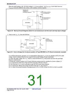
This characteristic is shown in figure 21.
The OVP terminal input current in the voltage lower than the OVP threshold voltage is based on I2 and the input current
in the voltage higher than the OVP threshold voltage is the sum of the current flowing to the base of Q3 and the current
flowing from the collector of Q2 to the base.
For holding in the latch state, it is necessary that the OVP terminal voltage is kept in the voltage higher than VBE of Q3.
So if the capacitor is connected between the OVP terminal and GND, even though Q2 turns on in a moment by the
surge voltage, etc. this latch action does not hold if the OVP terminal voltage does not become higher than VBE of Q3
by charging this capacitor.
For resetting OVP state, it is necessary to make the OVP terminal voltage lower than the OVP L threshold voltage or
make VCC lower than the OVP reset supply voltage.
REJ03D0835-0300 Rev.3.00 Jun 06, 2008
Page 26 of 40

 RENESAS [ RENESAS TECHNOLOGY CORP ]