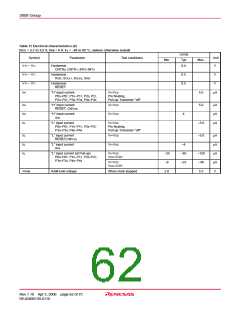
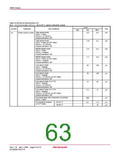
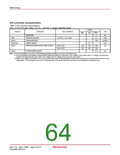
3858 Group
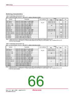
Switching characteristics
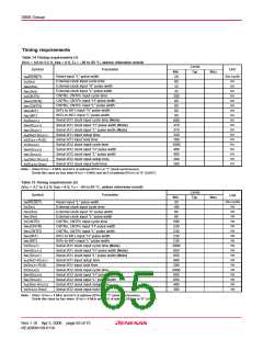
Table 16 Switching characteristics (1)
(VCC = 4.0 to 5.5 V, VSS = 0 V, Ta = –20 to 85 °C, unless otherwise noted)
Limits
Symbol
Parameter
Test conditions
Unit
Min.
Typ.
Max.
140
tWH (SCLK1)
tWL (SCLK1)
td (SCLK1-TXD)
tv (SCLK1-TXD)
tr (SCLK1)
tC(SCLK1)/2–30
tC(SCLK1)/2–30
Serial I/O1 clock output “H” pulse width
Serial I/O1 clock output “L” pulse width
Serial I/O1 output delay time (Note 1)
Serial I/O1 output valid time (Note 1)
Serial I/O1 clock output rising time
Serial I/O1 clock output falling time
Serial I/O2 clock output “H” pulse width
Serial I/O2 clock output “L” pulse width
Serial I/O2 output delay time (Note 2)
Serial I/O2 output valid time (Note 2)
Serial I/O2 clock output falling time
CMOS output rising time (Note 3)
CMOS output falling time (Note 3)
ns
ns
ns
ns
ns
ns
ns
ns
ns
ns
ns
ns
ns
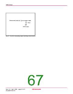
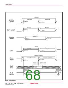
Fig. 61
–30
30
30
tf (SCLK1)
tWH (SCLK2)
tWL (SCLK2)
td (SCLK2-SOUT2)
tv (SCLK2-SOUT2)
tf (SCLK2)
tC(SCLK2)/2–160
tC(SCLK2)/2–160
200
0
30
30
30
tr (CMOS)
10
10
tf (CMOS)
Notes 1: When the P25/TXD P-channel output disable bit of the UART control register (bit 4 of address 001B16) is “0”.
2: When the P01/SOUT2 and P02/SCLK2 P-channel output disable bit of the Serial I/O2 control register 1 (bit 7 of address 001516) is “0”.
3: The XOUT pin is excluded.
Table 17 Switching characteristics (2)
(VCC = 2.7 to 5.5 V, VSS = 0 V, Ta = –20 to 85 °C, unless otherwise noted)
Limits
Symbol
Unit
Parameter
Test conditions
Min.
Typ.
Max.
350
Serial I/O1 clock output “H” pulse width
Serial I/O1 clock output “L” pulse width
Serial I/O1 output delay time (Note 1)
Serial I/O1 output valid time (Note 1)
Serial I/O1 clock output rising time
Serial I/O1 clock output falling time
Serial I/O2 clock output “H” pulse width
Serial I/O2 clock output “L” pulse width
Serial I/O2 output delay time (Note 2)
Serial I/O2 output valid time (Note 2)
Serial I/O2 clock output falling time
CMOS output rising time (Note 3)
CMOS output falling time (Note 3)
tC(SCLK1)/2–50
tC(SCLK1)/2–50
ns
ns
ns
ns
ns
ns
ns
ns
ns
ns
ns
ns
ns
tWH (SCLK1)
tWL (SCLK1)
td (SCLK1-TXD)
tv (SCLK1-TXD)
tr (SCLK1)
Fig. 61
–30
50
50
tf (SCLK1)
tC(SCLK2)/2–240
tC(SCLK2)/2–240
tWH (SCLK2)
tWL (SCLK2)
td (SCLK2-SOUT2)
tv (SCLK2-SOUT2)
tf (SCLK2)
400
0
50
50
50
20
20
tr (CMOS)
tf (CMOS)
Notes 1: When the P25/TXD P-channel output disable bit of the UART control register (bit 4 of address 001B16) is “0”.
2: When the P01/SOUT2 and P02/SCLK2 P-channel output disable bit of the Serial I/O2 control register 1 (bit 7 of address 001516) is “0”.
3: The XOUT pin is excluded.
Rev.1.10 Apr 3, 2006 page 66 of 75
REJ03B0139-0110

 RENESAS [ RENESAS TECHNOLOGY CORP ]