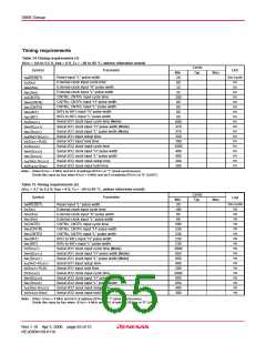
3858 Group
Timing requirements
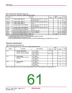
Table 14 Timing requirements (1)
(VCC = 4.0 to 5.5 V, VSS = 0 V, Ta = –20 to 85 °C, unless otherwise noted)
Limits
Typ.
Symbol
Parameter
Unit
Min.
20
Max.
Reset input “L” pulse width
XIN cycle
ns
tW(RESET)
tC(XIN)
External clock input cycle time
80
External clock input “H” pulse width
External clock input “L” pulse width
CNTR0, CNTR1 input cycle time
CNTR0, CNTR1 input “H” pulse width
CNTR0, CNTR1 input “L” pulse width
INT0 to INT3 input “H” pulse width
INT0 to INT3 input “L” pulse width
Serial I/O1 clock input cycle time (Note)
Serial I/O1 clock input “H” pulse width (Note)
Serial I/O1 clock input “L” pulse width (Note)
Serial I/O1 input setup time
32
ns
tWH(XIN)
32
ns
tWL(XIN)
200
80
ns
tC(CNTR)
ns
tWH(CNTR)
tWL(CNTR)
tWH(INT)
80
ns
80
ns
80
ns
tWL(INT)
800
370
370
220
100
1000
400
400
200
200
ns
tC(SCLK1)
ns
tWH(SCLK1)
tWL(SCLK1)
tsu(RxD-SCLK1)
th(SCLK1-RxD)
tC(SCLK2)
ns
ns
ns
Serial I/O1 input hold time
ns
Serial I/O2 clock input cycle time
Serial I/O2 clock input “H” pulse width
Serial I/O2 clock input “L” pulse width
Serial I/O2 clock input setup time
Serial I/O2 clock input hold time
ns
tWH(SCLK2)
tWL(SCLK2)
tsu(SIN2-SCLK2)
th(SCLK2-SIN2)
ns
ns
ns
Note : When f(XIN) = 8 MHz and bit 6 of address 001A16 is “1” (clock synchronous).
Divide this value by four when f(XIN) = 8 MHz and bit 6 of address 001A16 is “0” (UART).
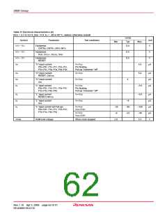
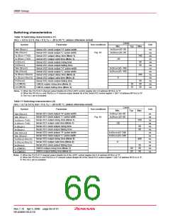
Table 15 Timing requirements (2)
(VCC = 2.7 to 5.5 V, VSS = 0 V, Ta = –20 to 85 °C, unless otherwise noted)
Limits
Typ.
Symbol
Parameter
Unit
Min.
20
Max.
XIN cycle
ns
tW(RESET)
tC(XIN)
Reset input “L” pulse width
External clock input cycle time
166
66
ns
tWH(XIN)
External clock input “H” pulse width
External clock input “L” pulse width
CNTR0, CNTR1 input cycle time
CNTR0, CNTR1 input “H” pulse width
CNTR0, CNTR1 input “L” pulse width
INT0 to INT3 input “H” pulse width
INT0 to INT3 input “L” pulse width
Serial I/O1 clock input cycle time (Note)
Serial I/O1 clock input “H” pulse width (Note)
Serial I/O1 clock input “L” pulse width (Note)
Serial I/O1 input setup time
ns
tWL(XIN)
66
ns
tC(CNTR)
500
230
230
230
230
2000
950
950
400
200
2000
950
950
400
300
ns
tWH(CNTR)
tWL(CNTR)
tWH(INT)
ns
ns
ns
tWL(INT)
ns
tC(SCLK1)
ns
tWH(SCLK1)
tWL(SCLK1)
tsu(RxD-SCLK1)
th(SCLK1-RxD)
tC(SCLK2)
ns
ns
ns
Serial I/O1 input hold time
ns
Serial I/O2 clock input cycle time
Serial I/O2 clock input “H” pulse width
Serial I/O2 clock input “L” pulse width
Serial I/O2 clock input setup time
Serial I/O2 clock input hold time
ns
tWH(SCLK2)
tWL(SCLK2)
tsu(SIN2-SCLK2)
th(SCLK2-SIN2)
ns
ns
ns
Note : When f(XIN) = 4 MHz and bit 6 of address 001A16 is “1” (clock synchronous).
Divide this value by four when f(XIN) = 4 MHz and bit 6 of address 001A16 is “0” (UART).
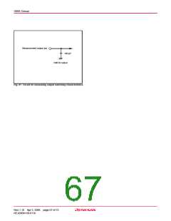
Rev.1.10 Apr 3, 2006 page 65 of 75
REJ03B0139-0110

 RENESAS [ RENESAS TECHNOLOGY CORP ]