3858 Group
TIMERS
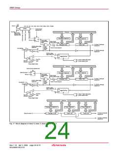
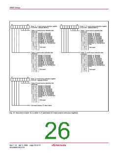
Timer X and Timer Y
■8-bit Timers
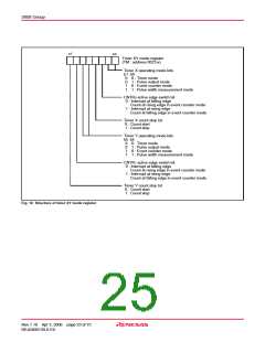
The timer X and timer Y can each select one of four operating
The 3858 group has four 8-bit timers: timer 1, timer 2, timer X, and
modes by setting the timer XY mode register (address 002316).
timer Y.
The timer 1 and timer 2 use one prescaler in common, and the
timer X and timer Y use each prescaler. Those are 8-bit
prescalers. Each of the timers and prescalers has a timer latch or
a prescaler latch.
(1) Timer mode
■Mode selection
This mode can be selected by setting “00” to the timer X operating
mode bits (bits 1 and 0) and the timer Y operating mode bits (bits
5 and 4) of the timer XY mode register (address 002316).
The division ratio of each timer or prescaler is given by 1/(n + 1),
where n is the value in the corresponding timer or prescaler latch.
All timers are down-counters. When the timer reaches “0016”, an
underflow occurs at the next count pulse and the contents of the
corresponding timer latch are reloaded into the timer and the
count is continued. When the timer underflows, the interrupt re-
quest bit corresponding to that timer is set to “1”.
■Explanation of operation
The timer count operation is started by setting “0” to the timer X
count stop bit (bit 3) and the timer Y count stop bit (bit 7) of the
timer XY mode register (address 002316).
When the timer reaches “0016”, an underflow occurs at the next
count pulse and the contents of timer latch are reloaded into the
timer and the count is continued.
■Timer divider
The divider count source is switched by the main clock division
ratio selection bits of CPU mode register (bits 7 and 6 at address
003B16). When these bits are “00” (high-speed mode) or “01”
(middle-speed mode), XIN is selected. When these bits are“10”
(low-speed mode), XCIN is selected.
(2) Pulse output mode
■Mode selection
This mode can be selected by setting “01” to the timer X operating
mode bits (bits 1 and 0) and the timer Y operating mode bits (bits
5 and 4) of the timer XY mode register (address 002316).
■Explanation of operation
■Prescaler 12
The prescaler 12 counts the output of the timer divider. The count
source is selected by the timer 12, X count source selection
register (address 002E16) among 1/2, 1/4, 1/8, 1/16, 1/32, 1/64, 1/
128, 1/256, 1/512, 1/1024 of f(XIN) or f(XCIN).
The operation is the same as the timer mode’s. Moreover the
pulse which is inverted each time the timer underflows is output
from CNTR0/CNTR1 pin. Regardless of the timer counting or not
the output of CNTR0/CNTR1 pin is initialized to the level of speci-
fied by their active edge switch bits when writing to the timer.
When the CNTR0 active edge switch bit (bit 2) and the CNTR1 ac-
tive edge switch bit (bit 6) of the timer XY mode register (address
002316) is “0”, the output starts with “H” level. When it is “1”, the
output starts with “L” level.
Timer 1 and Timer 2
The timer 1 and timer 2 counts the output of prescaler 12 and pe-
riodically set the interrupt request bit.
■Prescaler X and prescaler Y
Switching the CNTR0 or CNTR1 active edge switch bit will reverse
the output level of the corresponding CNTR0 or CNTR1 pin.
■Precautions
The prescaler X and prescaler Y count the output of the timer
divider or f(XCIN). The count source is selected by the timer 12, X
count source selection register (address 002E16) and the timer Y,
Z1 count source selection register (address 002F16) among 1/2,
1/4, 1/8, 1/16, 1/32, 1/64, 1/128, 1/256, 1/512, and 1/1024 of f(XIN)
or f(XCIN); and f(XCIN).
Set the double-function port of CNTR0/CNTR1 pin and port P27/
P40 to output in this mode.
Rev.1.10 Apr 3, 2006 page 22 of 75
REJ03B0139-0110

 RENESAS [ RENESAS TECHNOLOGY CORP ]