3858 Group
(3) Event counter mode
■Mode selection
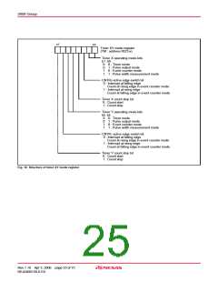
This mode can be selected by setting “10” to the timer X operating
mode bits (bits 1 and 0) and the timer Y operating mode bits (bits
5 and 4) of the timer XY mode register (address 002316).
■Explanation of operation
The operation is the same as the timer mode’s except that the
timer counts signals input from the CNTR0 or CNTR1 pin. The
valid edge for the count operation depends on the CNTR0 active
edge switch bit (bit 2) or the CNTR1 active edge switch bit (bit 6)
of the timer XY mode register (address 002316). When it is “0”, the
rising edge is valid. When it is “1”, the falling edge is valid.
■Precautions
Set the double-function port of CNTR0/CNTR1 pin and port P27/
P40 to input in this mode.
(4) Pulse width measurement mode
■Mode selection
This mode can be selected by setting “11” to the timer X operating
mode bits (bits 1 and 0) and the timer Y operating mode bits (bits
5 and 4) of the timer XY mode register (address 002316).
■Explanation of operation
When the CNTR0 active edge switch bit (bit 2) or the CNTR1 ac-
tive edge switch bit (bit 6) of the timer XY mode register (address
002316) is “1”, the timer counts during the term of one falling edge
of CNTR0/CNTR1 pin input until the next rising edge of input (“L”
term). When it is “0”, the timer counts during the term of one rising
edge input until the next falling edge input (“H” term).
■Precautions
Set the double-function port of CNTR0/CNTR1 pin and port P27/
P40 to input in this mode.
The count operation can be stopped by setting “1” to the timer X
count stop bit (bit 3) and the timer Y count stop bit (bit 7) of the
timer XY mode register (address 002316). The interrupt request bit
is set to “1” each time the timer underflows.
•Precautions when switching count source
When switching the count source by the timer 12, X and Y count
source selection bits, the value of timer count is altered in incon-
siderable amount owing to generating of thin pulses on the count
input signals.
Therefore, select the timer count source before setting the value
to the prescaler and the timer.
Rev.1.10 Apr 3, 2006 page 23 of 75
REJ03B0139-0110

 RENESAS [ RENESAS TECHNOLOGY CORP ]