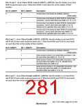
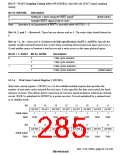
Bit 15—WAIT Sampling Timing Select (WAITSEL): Specifies the WAIT signal sampling
timing.
Bit 15: WAITSEL
Description
*
0
1
Setting to 1 when using the WAIT signal
Sampled WAIT signal at fall of CKIO
(Initial value)
Note: * Operation is not guaranteed if WAIT is asserted while WEITSEL = 0.
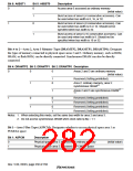
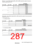
Bits 14, 3, and 2 —Reserved: These bits are always read as 0. The write value should always be
0.
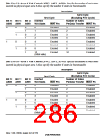
Bits 2n + 1, 2n—Area n (6–2, 0) Intercycle Idle Specification (AnIW1, AnIW0): Specify the
number of idles inserted between bus cycles when switching between physical space area n (6–2,
0) and another space or between a read access and a write access in the same physical space.
Bit 2n + 1: AnIW1 Bit 2n: AnIW0
Description
0
0
1
0
1
1 idle cycle inserted
1 idle cycle inserted
2 idle cycles inserted
3 idle cycles inserted
1
(Initial value)
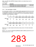
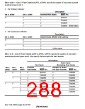
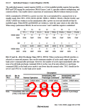
10.2.4 Wait State Control Register 2 (WCR2)
Wait state control register 2 (WCR2) is a 16-bit readable/writable register that specifies the
number of wait state cycles inserted for each area. It also specifies the data access pitch for burst
memory accesses. This allows direct connection of even low-speed memories without an external
circuit. WCR2 is initialized to H'FFFF by a power-on reset. It is not initialized by a manual reset
or in standby mode.
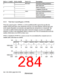
Bit:
15
14
13
12
11
10
9
8
A6 W2 A6 W1 A6 W0 A5 W2 A5 W1 A5 W0 A4 W2 A4 W1
Initial value:
R/W:
1
1
1
1
1
1
1
1
R/W
R/W
R/W
R/W
R/W
R/W
R/W
R/W
Bit:
7
6
5
4
3
2
1
0
A4 W0 A3 W1 A3 W0 A2 W1 A2 W0 A0 W2 A0 W1 A0 W0
Initial value:
R/W:
1
1
1
1
1
1
1
1
R/W
R/W
R/W
R/W
R/W
R/W
R/W
R/W
Rev. 5.00, 09/03, page 241 of 760

 RENESAS [ RENESAS TECHNOLOGY CORP ]