If a parity error occurs, however, the receiving station outputs an error signal (DE, low-level)
to request retransmission of the data. After outputting the error signal for the prescribed length
of time, the receiving station places the signal line in the high-impedance state again. The
signal line is pulled high again by a pull-up resistor.
5. If the transmitting station does not receive an error signal, it proceeds to transmit the next data
frame.
If it receives an error signal, however, it returns to step 2 and retransmits the erroneous data.
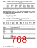
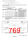
17.3.4 Register Settings
Table 17.3 shows a bit map of the registers used by the smart card interface. Bits indicated as 0 or
1 must be set to the value shown. The setting of other bits is described below.
Table 17.3 Smart Card Interface Register Settings
Bit
Register
SCSMR1
SCBRR1
SCSCR1
SCTDR1
SCSSR1
SCRDR1
SCSCMR1
Bit 7
GM
Bit 6
0
Bit 5
1
Bit 4
O/(
Bit 3
1
Bit 2
0
Bit 1
CKS1
BRR1
CKE1
TDR1
0
Bit 0
CKS0
BRR0
CKE0
TDR0
0
BRR7
TIE
BRR6
RIE
BRR5
TE
BRR4
BRR3
0
BRR2
0
RE
TDR7
TDRE
RDR7
—
TDR6
RDRF
RDR6
—
TDR5
ORER
RDR5
—
TDR4
TDR3
TDR2
TEND
RDR2
SINV
FER/ERS PER
RDR4
—
RDR3
SDIR
RDR1
—
RDR0
SMIF
SCSPTR1 EIO
—
—
—
SPB1IO SPB1DT SPB0IO SPB0DT
Note: A dash indicates an unused bit.
Serial Mode Register (SCSMR1) Settings: The GM bit is used to select the timing of TEND flag
setting, and, together with the CKE1 and CKE0 bits in the serial control register (SCSCR1), to
select the clock output state.
The O/( bit is cleared to 0 if the IC card is of the direct convention type, and set to 1 if of the
inverse convention type.
Bits CKS1 and CKS0 select the clock source of the on-chip baud rate generator. See section
17.3.5, Clock.
Rev. 6.0, 07/02, page 713 of 986

 RENESAS [ RENESAS TECHNOLOGY CORP ]