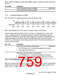
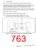
17.3.2 Pin Connections
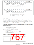
Figure 17.2 shows a schematic diagram of smart card interface related pin connections.
In communication with an IC card, since both transmission and reception are carried out on a
single data transmission line, the TxD pin and RxD pin should be connected outside the chip. The
data transmission line should be pulled up on the VCC power supply side with a resistor.
When the clock generated on the smart card interface is used by an IC card, the SCK pin output is
input to the CLK pin of the IC card. No connection is needed if the IC card uses an internal clock.
Chip port output is used as the reset signal.
Other pins must normally be connected to the power supply or ground.
Note: If an IC card is not connected, and both TE and RE are set to 1, closed
transmission/reception is possible, enabling self-diagnosis to be carried out.
VCC
TxD
IO
Data line
RxD
SCK
Clock line
Reset line
CLK
RST
SH7750
Series
Px (port)
IC card
Connected equipment
Figure 17.2 Schematic Diagram of Smart Card Interface Pin Connections
Rev. 6.0, 07/02, page 711 of 986

 RENESAS [ RENESAS TECHNOLOGY CORP ]