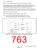
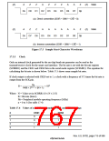
(Z)
A
Z
Z
A
Z
Z
Z
A
A
Z
(Z) State
Ds
D0
D1
D2
D3
D4
D5
D6
D7
Dp
(a) Direct convention (SDIR = SINV = O/ = 0)
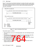
(Z)
A
Z
Z
A
A
A
A
A
A
Z
(Z) State
Ds
D7
D6
D5
D4
D3
D2
D1
D0
Dp
(b) Inverse convention (SDIR = SINV = O/ = 1)
Figure 17.5 Sample Start Character Waveforms
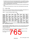
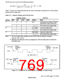
17.3.5 Clock
Only an internal clock generated by the on-chip baud rate generator can be used as the
transmit/receive clock for the smart card interface. The bit rate is set with the bit rate register
(SCBRR1) and the CKS1 and CKS0 bits in the serial mode register (SCSMR1). The equation for
calculating the bit rate is shown below. Table 17.5 shows some sample bit rates.
If clock output is selected with CKE0 set to 1, a clock with a frequency of 372 times the bit rate is
output from the SCK pin.
P
φ
B =
× 106
1488 × 22n–1 × (N + 1)
Where: N = Value set in SCBRR1 (0 ≤ N ≤ 255)
B = Bit rate (bits/s)
Pφ = Peripheral module operating frequency (MHz)
n = 0 to 3 (See table 17.4)
Table 17.4 Values of n and Corresponding CKS1 and CKS0 Settings
n
0
1
2
3
CKS1
CKS0
0
0
1
1
0
1
0
1
Rev. 6.0, 07/02, page 715 of 986

 RENESAS [ RENESAS TECHNOLOGY CORP ]