The bit rate error is given by the following equation:
φ
P
× 106 – 1 × 100
Error (%) =
1488 × 22n–1 × B × (N + 1)
Table 17.8 shows the relationship between the smart card interface transmit/receive clock register
settings and the output state.
Table 17.8 Register Settings and SCK Pin State
Register Values
SCK Pin
State
Setting
SMIF
GM
CKE1 CKE0
Output
1
*
1
1
0
0
0
Port
Determined by setting of SPB1IO
and SPB1DT bits in SCSPTR1
1
1
1
1
1
0
1
1
1
1
0
0
0
1
1
1
0
1
0
1
SCK (serial clock) output state
Low-level output state
2
2
*
*
2
3
Low output
High output
SCK (serial clock) output state
High-level output state
SCK (serial clock) output state
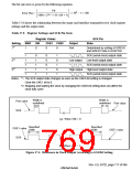
Notes: *1 The SCK output state changes as soon as the CKE0 bit setting is changed.
Clear the CKE1 bit to 0.
*2 Stopping and starting the clock by changing the CKE0 bit setting does not affect the
clock duty cycle.
Width is
undefined
Width is
undefined
Port value
SCK
Port value
(a) When GM = 0
Specified
width
Specified
width
CKE1 value
SCK
CKE1 value
(b) When GM = 1
Figure 17.6 Difference in Clock Output According to GM Bit Setting
Rev. 6.0, 07/02, page 717 of 986

 RENESAS [ RENESAS TECHNOLOGY CORP ]