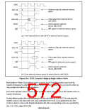
CHCRn.TS. In this process, the transfer data is temporarily stored in the data buffer in the bus
state controller (BSC).
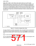
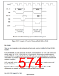
In a transfer between external memories such as that shown in figure 14.7, data is read from
external memory into the BSC’s data buffer in the read cycle, then written to the other external
memory in the write cycle. Figure 14.8 shows the timing for this operation. The DACK output
timing is the same as that of &6Q in a read or write cycle specified by the CHCRn.AM bit.
SAR
DAR
Memory
DMAC
Transfer source
module
Transfer destination
module
Data buffer
BSC
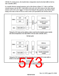
Taking the SAR value as the address, data is read from the transfer source module
and stored temporarily in the data buffer in the bus state controller (BSC).
1st bus cycle
SAR
DAR
Memory
DMAC
BSC
Transfer source
module
Transfer destination
module
Data buffer
Taking the DAR value as the address, the data stored in the BSC’s data buffer is
written to the transfer destination module.
2nd bus cycle
Figure 14.7 Operation in Dual Address Mode
Rev. 6.0, 07/02, page 521 of 986

 RENESAS [ RENESAS TECHNOLOGY CORP ]