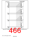
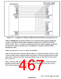
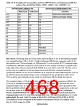
Table 13.16 Example of Correspondence between SH7750 Series and Synchronous DRAM
Address Pins (64-Bit Bus Width, AMX2–AMX0 = 011, AMXEXT = 0)
SH7750 Series Address Pin
RAS Cycle CAS Cycle
Synchronous DRAM Address Pin
Function
A14
A13
A12
A11
A10
A9
A22
A21
A20
A19
A18
A17
A16
A15
A14
A13
A12
A11
—
A22
H/L
0
A11
A10
A9
BANK select bank address
Address precharge setting
0
A8
A10
A9
A8
A7
A6
A5
A4
A3
A2
A1
A0
A7
A6
A8
A5
A7
A4
A6
A3
A5
A2
A4
A1
A3
A0
A2
Not used
Not used
Not used
A1
—
A0
—
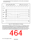
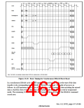
Burst Read: The timing chart for a burst read is shown in figure 13.28. In the following example
it is assumed that four 512k × 16-bit × 2-bank synchronous DRAMs are connected, and a 64-bit
data width is used. The burst length is 4. Following the Tr cycle in which ACTV command output
is performed, a READA command is issued in the Tc1 cycle, and the read data is accepted on the
rising edge of the external command clock (CKIO) from cycle Td1 to cycle Td4. The Tpc cycle is
used to wait for completion of auto-precharge based on the READA command inside the
synchronous DRAM; no new access command can be issued to the same bank during this cycle. In
the SH7750 Series, the number of Tpc cycles is determined by the specification of bits TPC2–
TPC0 in MCR, and commands are not issued for synchronous DRAM during this interval.
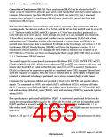
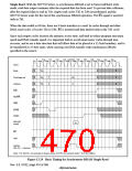
The example in figure 13.28 shows the basic cycle. To connect slower synchronous DRAM, the
cycle can be extended by setting WCR2 and MCR bits. The number of cycles from the ACTV
command output cycle, Tr, to the READA command output cycle, Tc1, can be specified by bits
RCD1 and RCD0 in MCR, with a value of 0 to 3 specifying 2 to 4 cycles, respectively. In the case
of 2 or more cycles, a Trw cycle, in which an NOP command is issued for the synchronous
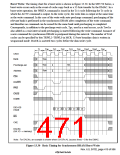
DRAM, is inserted between the Tr cycle and the Tc cycle. The number of cycles from READA
command output cycle Tc1 to the first read data latch cycle, Td1, can be specified as 1 to 5 cycles
independently for areas 2 and 3 by means of bits A2W2–A2W0 and A3W2–A3W0 in WCR2.
This number of cycles corresponds to the number of synchronous DRAM CAS latency cycles.
Rev. 6.0, 07/02, page 416 of 986

 RENESAS [ RENESAS TECHNOLOGY CORP ]