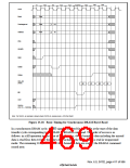
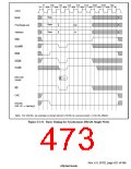
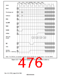
Single Write: The basic timing chart for write access is shown in figure 13.31. In a single write
operation, following the Tr cycle in which ACTV command output is performed, a WRITA
command that performs auto-precharge is issued in the Tc1 cycle. In the write cycle, the write data
is output at the same time as the write command. In the case of a write with auto-precharge,
precharging of the relevant bank is performed in the synchronous DRAM after completion of the
write command, and therefore no command can be issued for synchronous DRAM until
precharging is completed. Consequently, in addition to the precharge wait cycle, Tpc, used in a
read access, cycle Trwl is also added as a wait interval until precharging is started following the
write command. Issuance of a new command for synchronous DRAM is postponed during this
interval. The number of Trwl cycles can be specified by bits TRWL2–TRWL0 in MCR. DACK is
asserted two cycles before the data write cycle.
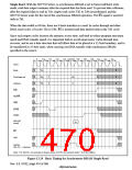
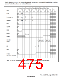
As the SH7750 Series supports burst read/burst write operations for synchronous DRAM, there
are empty cycles in a single write operation.
Rev. 6.0, 07/02, page 420 of 986

 RENESAS [ RENESAS TECHNOLOGY CORP ]