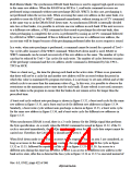
Single Read: With the SH7750 Series, as synchronous DRAM is set to burst read/burst write
mode, read data output continues after the required data has been read. To prevent data collisions,
after the required data is read in Td1, empty read cycles Td2 to Td4 are performed, and the
SH7750 Series waits for the end of the synchronous DRAM operation. The %6 signal is asserted
only in Td1.
When the data width is 64 bits, there are 4 burst transfers in a read. In cache-through and other
DMA read cycles, of cycles Td1 to Td4, %6 is asserted and data latched only in the Td1 cycle.
Since such empty cycles increase the memory access time, and tend to reduce program execution
speed and DMA transfer speed, it is important both to avoid unnecessary cache-through area
accesses, and to use a data structure that will allow data to be placed at a 32-byte boundary, and to
be transferred in 32-byte units, when carrying out DMA transfer with synchronous DRAM
specified as the source.
Tr
Trw
Tc1
Tc2
Tc3 Tc4/Td1 Td2
Td3
Td4
Tpc
Tpc
Tpc
CKIO
Bank
Row
Row
Row
Precharge-sel
Address
H/L
c1
RD/
DQMn
D63–D0
(read)
c1
CKE
DACKn
(SA: IO ← memory)
Note: For DACKn, an example is shown where CHCRn.AL (access level) = 0 for the DMAC.
Figure 13.29 Basic Timing for Synchronous DRAM Single Read
Rev. 6.0, 07/02, page 418 of 986

 RENESAS [ RENESAS TECHNOLOGY CORP ]