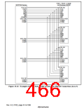
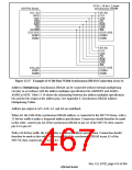
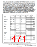
512k × 16-bit × 2-bank
synchronous DRAM
SH7750 Series
A11–A2
CKIO
CKE
A9–A0
CLK
CKE
RD/
D31–D16
DQM3
DQM2
I/O15–I/O0
DQMU
DQML
A9–A0
CLK
CKE
I/O15–I/O0
DQMU
DQML
D15–D0
DQM1
DQM0
Figure 13.27 Example of 32-Bit Data Width Synchronous DRAM Connection (Area 3)
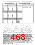
Address Multiplexing: Synchronous DRAM can be connected without external multiplexing
circuitry in accordance with the address multiplex specification bits AMXEXT and AMX2–
AMX0 in MCR. Table 13.16 shows the relationship between the address multiplex specification
bits and the bits output at the address pins. See Appendix F, Synchronous DRAM Address
Multiplexing Tables.
Address pin output at A25–A18, A1, and A0 are undefined.
When A0, the LSB of the synchronous DRAM address, is connected to the SH7750 Series, with a
32-bit bus width it makes a longword address specification. Connection should therefore be made
in this order: connect pin A0 of the synchronous DRAM to pin A2 of the SH7750, then connect
pin A1 to pin A3.
With a 64-bit bus width, the LSB makes a quadword address specification. Connection should
therefore be made in this order: connect pin A0 of the synchronous DRAM to pin A3 of the
SH7750, then connect pin A1 to pin A4.
Rev. 6.0, 07/02, page 415 of 986

 RENESAS [ RENESAS TECHNOLOGY CORP ]