13.3.5 Synchronous DRAM Interface
Connection of Synchronous DRAM: Since synchronous DRAM can be selected by the &6
signal, it can be connected to physical space areas 2 and 3 using 5$6 and other control signals in
common. If the memory type bits (DRAMTP2–0) in BCR1 are set to 010, area 2 is normal
memory space and area 3 is synchronous DRAM space; if set to 011, areas 2 and 3 are both
synchronous DRAM space.
With the SH7750 Series, burst read/burst write mode is supported as the synchronous DRAM
operating mode. The data bus width is 32 or 64 bits, and the SZ size bits in MCR must be set to 00
or 11. The burst enable bit (BE) in MCR is ignored, a 32-byte burst transfer is performed in a
cache fill/copy-back cycle, and in a write-through area write or a non-cacheable area read/write,
32-byte data is read even in a single read in order to access synchronous DRAM with a burst
read/write access. 32-byte data transfer is also performed in a single write, but DQMn is not
asserted when unnecessary data is transferred. For details on the burst length, see section 13.2.10,
Synchronous DRAM Module Register (SDMR), and Power-On Sequence in section 13.3.5,
Synchronous DRAM Interface. For changing the burst length (a function only available in the
SH7750R) for a 32-bit bus, see Notes on Changing the Burst Length (SH7750R Only) in section
13.3.5, Synchronous DRAM Interface.
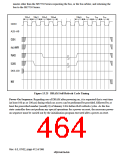
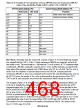
The control signals for connection of synchronous DRAM are 5$6, &$6, RD/:5, &65 or &66,
DQM0 to DQM7, and CKE. All the signals other than &65 and &66 are common to all areas, and
signals other than CKE are valid and latched only when &65 or &66 is asserted. Synchronous
DRAM can therefore be connected in parallel to a number of areas. CKE is negated (driven low)
when the frequency is changed, when the clock is unstable after the clock supply is stopped and
restarted, or when self-refreshing is performed, and is always asserted (high) at other times.
Commands for synchronous DRAM are specified by 5$6, &$6, RD/:5, and specific address
signals. The commands are NOP, auto-refresh (REF), self-refresh (SELF), precharge all banks
(PALL), precharge specified bank (PRE), row address strobe bank active (ACTV), read (READ),
read with precharge (READA), write (WRIT), write with precharge (WRITA), and mode register
setting (MRS).
Byte specification is performed by DQM0 to DQM7. A read/write is performed for the byte for
which the corresponding DQM signal is low. When the bus width is 64 bits, in big-endian mode
DQM7 specifies an access to address 8n, and DQM0 specifies an access to address 8n + 7. In
little-endian mode, DQM7 specifies an access to address 8n + 7, and DQM0 specifies an access to
address 8n.
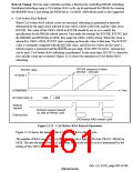
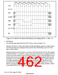
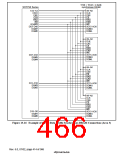
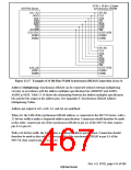
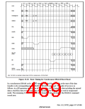
Figures 13.26 and 13.27 show examples of the connection of 16M × 16-bit synchronous DRAMs.
Rev. 6.0, 07/02, page 413 of 986

 RENESAS [ RENESAS TECHNOLOGY CORP ]