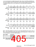
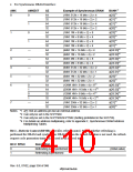
Bit 15: TRWL2
Bit 14: TRWL1
Bit 13: TRWL0
Write Precharge ACT Delay Time
0
0
0
1
0
1
0
1
0
1
1 (Initial value)
2
1
0
1
3*
4*
1
5*
Reserved (Setting prohibited)
Reserved (Setting prohibited)
Reserved (Setting prohibited)
Note: * Inhibited in RAS down mode.
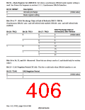
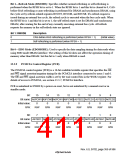
Bits 12 to 10—CAS-Before-RAS Refresh 5$6 Assertion Period (TRAS2–TRAS0): When the
DRAM interface is set, these bits set the 5$6 assertion period in CAS-before-RAS refreshing.
When the synchronous DRAM interface is set, the bank active command is not issued for a period
of TRC* + TRAS after an auto-refresh command is issued.
Note: * Bits 29 to 27: RAS precharge interval at end of refresh.
Command
Interval after
5$6/DRAM
Synchronous
Assertion Period DRAM Refresh
Bit 12: TRAS2
Bit 11: TRAS1
Bit 10: TRAS0
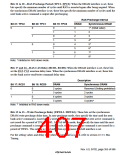
0
0
0
2
4 + TRC*
(Initial value)
1
0
1
0
1
0
1
3
4
5
6
7
8
9
5 + TRC
6 + TRC
7 + TRC
8 + TRC
9 + TRC
10 + TRC
11 + TRC
1
0
1
1
Note: * Bits 29 to 27: RAS precharge interval at end of refresh.
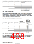
Bit 9—Burst Enable (BE): Specifies whether burst access is performed on DRAM interface. In
synchronous DRAM access, burst access is always performed regardless of the specification of
this bit. The DRAM transfer mode depends on EDOMODE.
Rev. 6.0, 07/02, page 356 of 986

 RENESAS [ RENESAS TECHNOLOGY CORP ]