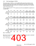
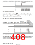
Bits 21 to 19—RAS Precharge Period (TPC2–TPC0): When the DRAM interface is set, these
bits specify the minimum number of cycles until 5$6 is asserted again after being negated. When
the synchronous DRAM interface is set, these bits specify the minimum number of cycles until the
next bank active command is output after precharging.
RAS Precharge Interval
Bit 21: TPC2
Bit 20: TPC1
Bit 19: TPC0
DRAM
Synchronous DRAM
0
0
0
1
0
1
0
1
0
1
0
1
2
3
4
5
6
7
1* (Initial value)
2
1
0
1
3
4*
5*
6*
7*
8*
1
Note: * Inhibited in RAS down mode.
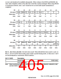
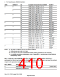
Bits 17 and 16—RAS-CAS Delay (RCD1, RCD0): When the DRAM interface is set, these bits
set the 5$6-&$6 assertion delay time. When the synchronous DRAM interface is set, these bits
set the bank active-read/write command delay time.
Description
Bit 17: RCD1
Bit 16: RCD0
DRAM
Synchronous DRAM
Reserved (Setting prohibited)
2 cycles
0
0
1
0
1
2 cycles
3 cycles
4 cycles
5 cycles
1
3 cycles
4 cycles*
Note: * Inhibited in RAS down mode.
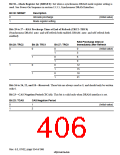
Bits 15 to 13—Write Precharge Delay (TRWL2–TRWL0): These bits set the synchronous
DRAM write precharge delay time. In auto-precharge mode, they specify the time until the next
bank active command is issued after a write cycle. After a write cycle, the next active command is
not issued for a period of TPC + TRWL. In RAS down mode, they specify the time until the next
precharge command is issued. After a write cycle, the next precharge command is not issued for a
period of TRWL. This setting is valid only when synchronous DRAM interface is set.
For the setting values and delay time when no command is issued, refer to section 22.3.3, Bus
Timing.
Rev. 6.0, 07/02, page 355 of 986

 RENESAS [ RENESAS TECHNOLOGY CORP ]