on reset, and should not be modified subsequently. When writing to bits RFSH and RMODE, the
same values should be written to the other bits so that they remain unchanged. When using DRAM
or synchronous DRAM, areas 2 and 3 should not be accessed until register initialization is
completed.
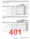
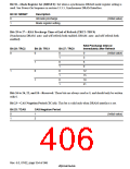
Bit:
31
30
29
28
TRC1
0
27
TRC0
0
26
—
0
25
—
0
24
—
0
Bit name: RASD MRSET TRC2
Initial value:
R/W:
0
0
0
R/W
R/W
R/W
R/W
R/W
R
R
R
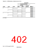
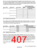
Bit:
23
22
—
0
21
TPC2
0
20
TPC1
0
19
TPC0
0
18
—
0
17
RCD1
0
16
RCD0
0
Bit name: TCAS
Initial value:
R/W:
0
R/W
R
R/W
R/W
R/W
R
R/W
R/W
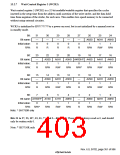
Bit:
15
14
13
12
11
10
9
BE
0
8
Bit name: TRWL2 TRWL1 TRWL0 TRAS2 TRAS1 TRAS0
SZ1
0
Initial value:
R/W:
0
0
0
0
0
0
R/W
R/W
R/W
R/W
R/W
R/W
R/W
R/W
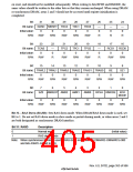
Bit:
7
6
5
4
3
2
1
0
Bit name:
SZ0 AMXEXT AMX2
AMX1
AMX0
RFSH RMODE EDO
MODE
Initial value:
R/W:
0
0
0
0
0
0
0
0
R/W
R/W
R/W
R/W
R/W
R/W
R/W
R/W
Bit 31—RAS Down (RASD): Sets RAS down mode. When DRAM/RAS down mode is used, set
BE to 1. Do not set RAS down mode in slave mode or partial-sharing mode, or when areas 2 and 3
are both designated as synchronous DRAM interface.
Bit 31: RASD
Description
0
1
Normal mode
RAS down mode
(Initial value)
Note: When synchronous DRAM is used in RAS down mode, set bits DMAIW2–DMAIW0 to 000
and bits A3IW2–A3IW0 to 000.
Rev. 6.0, 07/02, page 353 of 986

 RENESAS [ RENESAS TECHNOLOGY CORP ]