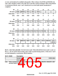
Bit 4n + 2—Area n (6 to 0) Write Strobe Setup Time (AnS0): Specifies the number of cycles
inserted in the setup time from the address until assertion of the read/write strobe. Valid only for
SRAM interface, byte control SRAM interface, and burst ROM interface.
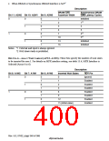
Bit 4n + 2: AnS0
Waits Inserted in Setup
0
1
0
1
(Initial value)
(n = 6 to 0)
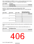
Bits 4n + 1 and 4n—Area n (6 to 0) Data Hold Time (AnH1, AnH0): When writing, these bits
specify the number of cycles to be inserted in the hold time from negation of the write strobe.
When reading, they specify the number of cycles to be inserted in the hold time from the data
sampling timing. Valid only for SRAM interface, byte control SRAM interface, and burst ROM
interface.
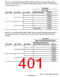
Bit 4n + 1: AnH1
Bit 4n: AnH0
Waits Inserted in Hold
0
0
1
0
1
0
1
2
3
1
(Initial value)
(n = 6 to 0)
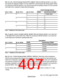
Bits 4n+3 Area n (4 or 1) Read-Strobe Negate Timing (AnRDH) (Setting Only Possible in
the SH7750R): When reading, these bits specify the timing for the negation of read strobe. These
bits should be cleared to 0 when a byte control SRAM setting is made.
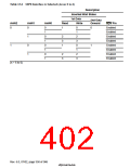
Bit 4n + 3: AnRDH
Read-Strobe Negate Timing
0
Negation occurs after insertion of the number of hold wait cycles specified
by the AnH setting
Negation occurs based on the read strobe data sampling timing
(n = 4 or 1)
(Initial value)
1
13.2.8 Memory Control Register (MCR)
The memory control register (MCR) is a 32-bit readable/writable register that specifies 5$6 and
&$6 timing and burst control for DRAM and synchronous DRAM (areas 2 and 3), address
multiplexing, and refresh control. This enables DRAM and synchronous DRAM to be connected
without using external circuitry.
MCR is initialized to H'00000000 by a power-on reset, but is not initialized by a manual reset or in
standby mode. Bits RASD, MRSET, TRC2–0, TPC2–0, RCD1–0, TRWL2–0, TRAS2–0, BE,
SZ1–0, AMXEXT, AMX2–0, and EDOMODE are written in the initialization following a power-
Rev. 6.0, 07/02, page 352 of 986

 RENESAS [ RENESAS TECHNOLOGY CORP ]