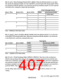
Bit 30—Mode Register Set (MRSET): Set when a synchronous DRAM mode register setting is
used. See Power-On Sequence in section 13.3.5, Synchronous DRAM Interface.
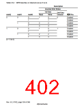
Bit 30: MRSET
Description
0
1
All-bank precharge
Mode register setting
(Initial value)
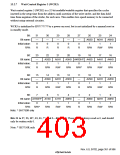
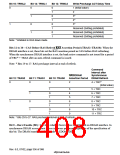
Bits 29 to 27—RAS Precharge Time at End of Refresh (TRC2–TRC0)
(Synchronous DRAM: auto- and self-refresh both enabled; DRAM: auto- and self-refresh both
enabled)
RAS Precharge Interval
Bit 29: TRC2
Bit 28: TRC1
Bit 27: TRC0
Immediately after Refresh
0
0
0
1
0
1
0
1
0
1
0
(Initial value)
3
1
0
1
6
9
1
12
15
18
21
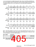
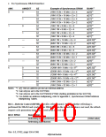
Bits 26 to 24, 22, and 18—Reserved: These bits are always read as 0, and should only be written
with 0.
Bit 23—CAS Negation Period (TCAS): This bit is valid only when DRAM interface is set.
Bit 23: TCAS
CAS Negation Period
0
1
1
2
(Initial value)
Rev. 6.0, 07/02, page 354 of 986

 RENESAS [ RENESAS TECHNOLOGY CORP ]