•
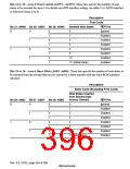
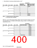
When DRAM or Synchronous DRAM Interface is Set*1
Description
Synchronous DRAM
DRAM &$6
Bit 11: A2W2 Bit 10: A2W1 Bit 9: A2W0
Assertion Width
&$6 Latency Cycles
0
1
0
1
0
1
0
1
0
1
0
1
0
1
1
Inhibited
2
*
2
1
2
3
4
5
3
4
2
2
*
*
7
10
13
16
Inhibited
Inhibited
Notes: *1 External wait input is always ignored.
*2 RAS down mode is prohibited.
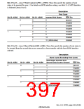
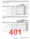
Bits 8 to 6—Area 1 Wait Control (A1W2–A1W0): These bits specify the number of wait states
to be inserted for area 1. For details on MPX interface setting, see table 13.6, MPX Interface is
Selected (Areas 0 to 6).
Description
Bit 8: A1W2
Bit 7: A1W1
Bit 6: A1W0
Inserted Wait States
5'< Pin
Ignored
Enabled
Enabled
Enabled
Enabled
Enabled
Enabled
Enabled
0
0
0
1
0
1
0
1
0
1
0
1
1
0
1
2
3
1
6
9
12
15 (Initial value)
Rev. 6.0, 07/02, page 348 of 986

 RENESAS [ RENESAS TECHNOLOGY CORP ]