•
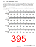
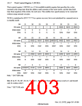
When DRAM or Synchronous DRAM Interface is Set*1
Description
Synchronous DRAM
DRAM &$6
Bit 15: A3W2 Bit 14: A3W1 Bit 13: A3W0
Assertion Width
&$6 Latency Cycles
0
1
0
1
0
1
0
1
0
1
0
1
0
1
1
Inhibited
2
*
2
1
2
3
4
5
3
4
2
2
*
*
7
10
13
16
Inhibited
Inhibited
Notes: *1 External wait input is always ignored.
*2 Inhibited in RAS down mode.
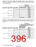
Bits 11 to 9—Area 2 Wait Control (A2W2–A2W0): These bits specify the number of wait states
to be inserted for area 2. External wait input is only enabled when the SRAM interface or MPX
interface is used, and is ignored when DRAM or synchronous DRAM is used. For details on MPX
interface setting, see table 13.6, MPX Interface is Selected (Areas 0 to 6).
•
When SRAM Interface is Set
Description
Inserted Wait States
Bit 11: A2W2 Bit 10: A2W1 Bit 9: A2W0
5'< Pin
Ignored
Enabled
Enabled
Enabled
Enabled
Enabled
Enabled
Enabled
0
0
1
0
1
0
1
0
1
0
1
0
1
0
1
2
3
1
6
9
12
15 (Initial value)
Rev. 6.0, 07/02, page 347 of 986

 RENESAS [ RENESAS TECHNOLOGY CORP ]