PULSE OUTPUT PORT MODE
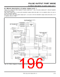
9.3 Block description of pulse output port 1
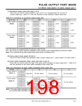
9.3.2 Pulse output data registers 0, 1
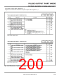
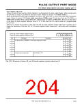
Figure 9.3.3 shows the structures of pulse output data registers 0, 1.
b7 b6 b5 b4 b3 b2 b1 b0
Pulse output data register 0 (Address A216
)
Bit
0
Bit name
Function
At reset R/W
RTP2
RTP2
RTP2
0
1
2
pulse output data bit
0
0
0
0
0
RW
RW
RW
RW
RW
0 : “L” level output
1 : “H” level output
pulse output data bit
pulse output data bit
1
2
3
RTP2
3
0
pulse output data bit
pulse output data bit
(Valid in pulse mode 1.) (Note)
RTP3
4
5
RTP3 pulse output data bit
(Valid in pulse mode 1.) (Note)
1
0
0
RW
RW
b7 b6
Pulse output trigger select bits
7, 6
0 0 : Underflow of timer A5
0 1 : Falling edge of input signal to pin RTPTRG1
1 0 : Rising edge of input signal to pin RTPTRG1
1 1 : Both falling and rising edges of input signal to
pin RTPTRG1
Note: Invalid in pulse mode 0.
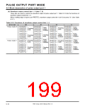
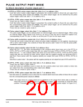
b7 b6 b5 b4 b3 b2 b1 b0
Pulse output data register 1 (Address A416
)
Bit
0
Bit name
Function
At reset R/W
Pulse width modulation enable
bit 0
0 : No pulse width modulation by timer A6
1 : Pulse width modulation by timer A6
0
0
0
0
0
RW
RW
RW
RW
RW
0 : No pulse width modulation by timer A7
1 : Pulse width modulation by timer A7
Pulse width modulation enable
bit 1
1
2
0 : No pulse width modulation by timer A9
1 : Pulse width modulation by timer A9
Pulse width modulation enable
bit 2
Pulse output polarity select bit
0 : Positive
1 : Negative
3
4
RTP3
0
pulse output data bit
(Valid in pulse mode 0) (Note)
0 : “L” level output
1 : “H” level output
5
RTP3 pulse output data bit
1
0
RW
(Valid in pulse mode 0) (Note)
6
7
0
0
RW
RW
RTP3
RTP3
2
3
pulse output data bit
pulse output data bit
Note: Invalid in pulse mode 1.
Fig. 9.3.3 Structures of pulse output data registers 0, 1
7905 Group User’s Manual Rev.1.0
9-19

 RENESAS [ RENESAS TECHNOLOGY CORP ]