PULSE OUTPUT PORT MODE
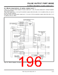
9.3 Block description of pulse output port 1
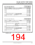
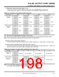
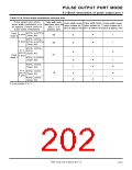
(1) Waveform output select bits (bits 2 to 0)
These bits are used to select whether a pin serves as a programmable I/O port pin or
a pulse output pin. Table 9.3.1 lists the functions of the waveform output select bits.
Table 9.3.1 Functions of waveform output select bits
001
010
b2 b1 b0
Pulse mode 0
(Note)
000
011
P4
P4
P4
P4
7
6
5
4
/RTP3
3
2
1
0
P4
P4
P4
P4
7
6
5
4
/RTP3
3
2
1
0
P4
P4
P4
P4
7
6
5
4
/RTP3
3
2
1
0
P4
P4
P4
P4
7
6
5
4
/RTP3
3
2
1
0
/RTP3
/RTP3
/RTP3
/RTP3
/RTP3
/RTP3
/RTP3
/RTP3
/RTP3
/RTP3
/RTP3
/RTP3
RTP
RTP
Port
Port
P4
P4
P4
P4
3
2
1
0
/RTP2
/RTP2
/RTP2
/RTP2
3
2
1
0
P4
P4
P4
P4
3
2
1
0
/RTP2
/RTP2
/RTP2
/RTP2
3
2
1
0
P4
P4
P4
P4
3
2
1
0
/RTP2
/RTP2
/RTP2
/RTP2
3
2
1
0
P4
P4
P4
P4
3
2
1
0
/RTP2
/RTP2
/RTP2
/RTP2
3
2
1
0
RTP
RTP
RTP
Port
Port
RTP
Port
Port
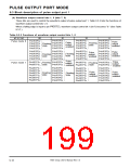
P4
P4
7
/RTP3
/RTP3
3
P4
P4
7
6
/RTP3
/RTP3
3
2
P4
P4
7
6
/RTP3
/RTP3
3
2
P4
P4
7
6
/RTP3
/RTP3
3
2
Pulse mode 1
6
2
(Note)
P4
P4
P4
P4
P4
P4
5
4
3
2
1
0
/RTP3
/RTP3
/RTP2
/RTP2
/RTP2
/RTP2
1
0
3
2
1
0
P4
P4
P4
P4
P4
P4
5
4
3
2
1
0
/RTP3
/RTP3
/RTP2
/RTP2
/RTP2
/RTP2
1
0
3
2
1
0
P4
P4
P4
P4
P4
P4
5
4
3
2
1
0
/RTP3
/RTP3
/RTP2
/RTP2
/RTP2
/RTP2
1
0
3
2
1
0
P4
P4
P4
P4
P4
P4
5
4
3
2
1
0
/RTP3
/RTP3
/RTP2
/RTP2
/RTP2
/RTP2
1
0
3
2
1
0
Port
RTP
RTP
Port
Port: This serves as a programmable I/O port pin or timer I/O pin.
RTP: This serves as a pulse output pin regardless of the contents of the corresponding port direction register.
Note: This is selected by the pulse output mode select bit (bit 3 at address A016).
(2) Pulse output mode select bit (bit 3)
This bit is used to select the operation mode of pulse output port 1: pulse mode 0 or pulse mode 1.
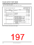
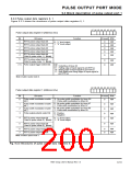
(3) Pulse width modulation timer select bits (bits 5 and 4)
These bits are used to select the type of the pulse width modulation of pulse output port 1. Table 9.3.2
lists the functions of the pulse width modulation timer select bits.
Table 9.3.2 Functions of pulse width modulation timer select bits
b5 b4
Pulse mode 0
(Note 1)
00
01
10
11
P4
P4
P4
P4
3
2
1
0
/RTP2
3
2
1
0
/RTP2
/RTP2
/RTP2
Do not select.
Timer A6
Timer A6
Do not select.
Do not select.
P4
P4
5
4
/RTP3
/RTP3
1
0
P4
P4
P4
5
4
3
/RTP3
/RTP3
/RTP2
1
0
3
P4
P4
P4
P4
P4
P4
5
4
3
2
1
0
/RTP3
/RTP3
/RTP2
/RTP2
/RTP2
/RTP2
1
0
3
2
1
0
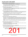
Pulse mode 1
Timer A9
Timer A7
Timer A6
Timer A7
Timer A6
(Note 2)
P4
P4
3
2
/RTP2
/RTP2
3
2
Do not select.
P4
P4
P4
2
1
0
/RTP2
/RTP2
/RTP2
2
1
0
P4
P4
1
0
/RTP2
/RTP2
1
0
Note 1: The pulse width modulation cannot be applied to pins RTP3
0
to RTP3
3
.
2: The pulse width modulation cannot be applied to pins RTP3
2
and RTP3 .
3
7905 Group User’s Manual Rev.1.0
9-17

 RENESAS [ RENESAS TECHNOLOGY CORP ]