PULSE OUTPUT PORT MODE
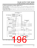
9.3 Block description of pulse output port 1
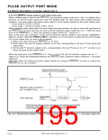
9.3 Block description of pulse output port 1
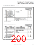
Figure 9.3.1 shows the block diagram of pulse output port 1. Also, the pulse-output-port-1-relevant registers
are described below.
After pulse output port 1 is set by the waveform output select bits (bits 2 to 0 at address A016), be sure to
set the relevant registers.
Note that, when not using pulse output port 1, be sure to fix the waveform output select bits (bits 2 to 0
at address A016) to “000 .”
2
Pulse width modulation timer select bits
(bits 5, 4 at address A016
)
Pulse width modulation
output of timer A6
Pulse output trigger select bits
Pulse width modulation
output of timer A7
Pulse width
modulation
circuit
(bits 7, 6 at address A216
)
Pulse width modulation
output of timer A9
RTPTRG1
Timer A5
Pulse width modulation enable bits
0 through 2
(bits 0 through 2 at address A416
)
Waveform output control bit 1
T
b0
(bit 7 at address A016
)
D
D
Q
Q
D Q
R
b1
b2
P4OUTCUT
D
Q
Bits 0 through 3 of pulse
output data register 0
Reset
(address A216
)
T
RTP2
RTP2
0
1
b0
b1
b2
b3
D
D
Q
Q
RTP2
RTP2
2
3
D
D
Q
Q
Pulse output mode
select bit
(bit 3 at address A016
)
T
RTP3
RTP3
0
1
b4
b5
D
D
Q
Q
Bits 4, 5 of pulse output data register 0
(address A216
)
or
Bits 4, 5 of pulse output data register 1
(address A416
)
D
D
Q
Q
b6
b7
RTP3
RTP3
2
3
T
Pulse output polarity
select bit
Waveform output
control bit 0
(bit 6 at address A016
Bits 6, 7 of pluse
output data register 1
(address A416
(bit 3 at address A416
)
)
)
D Q
R
Timer 8
Reset
Fig. 9.3.1 Block diagram of pulse output port 1
7905 Group User’s Manual Rev.1.0
9-15

 RENESAS [ RENESAS TECHNOLOGY CORP ]