PULSE OUTPUT PORT MODE
9.3 Block description of pulse output port 1
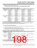
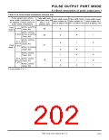
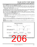
Table 9.3.4 Pulse-width-modulation-relevant bits
Pulse output pins where
pulse width modulation is to
be applied (Timers used for
pulse width modulation)
Pulse width modu-
lation timer select bits
(bits 5, 4 at
Pulse width modu-
lation enable bit 1
Pulse width modu-
lation enable bit 2
Pulse width modu-
lation enable bit 0
(bit 1 at address A416
)
(bit 0 at address A416
(bit 2 at address A416
)
)
address A016
)
RTP2
(Timer A6)
3
to RTP2
0
0
Pulse
mode
4 pins
6 pins
➀
1
00
➀
0
RTP3
RTP2
(Timer A6)
1
3
, RTP3
0
,
to RTP2
➀
1
00
01
➀
➀
RTP3
RTP2
(Timer A7)
1
3
, RTP3 ,
0
In a
unit of
1
➀
Pulse
mode
3 pins
1
RTP2
(Timer A6)
2
to RTP2
0
➀
➀
1
➀
RTP3
(Timer A9)
1
, RTP3
0
➀
1
In a
unit of
2 pins
RTP2
(Timer A7)
3
, RTP2
2
0
10
1
➀
➀
➀
RTP2 , RTP2
1
➀
1
(Timer A6)
X: It may be either “0” or “1.”
7905 Group User’s Manual Rev.1.0
9-21

 RENESAS [ RENESAS TECHNOLOGY CORP ]