PULSE OUTPUT PORT MODE
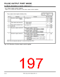
9.3 Block description of pulse output port 1
(1) RTP2
0
to RTP2 pulse output data bits (bits 0 to 3 at address A216)
3
Each time when a pulse output trigger is generated, the contents written to these bits are output from
the corresponding pulse output pins (Note). The pulse output trigger can be selected by the pulse
output trigger select bits (bits 7, 6 at address A216).
(2) RTP3
0
, RTP3 pulse output data bits (bits 4, 5 at address A216)
1
These bits are valid in pulse mode 1.
Each time when a pulse output trigger is generated, the contents written to these bits are output from
the corresponding pulse output pins (Note). The pulse output trigger can be selected by the pulse
output trigger select bits (bits 7, 6 at address A216).
These bits are invalid in pulse mode 0.
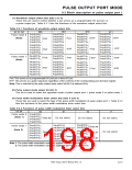
(3) Pulse output trigger select bits (bits 7, 6 at address A216
)
The pulse output trigger can be selected from an internal trigger and an external trigger. When using
an external trigger (input signal to pin RTPTRG1), be sure to clear the port P5 direction register’s bit,
corresponding to port P5
2
pin, in order to set this port P5 pin for the input mode.
2
(4) Pulse width modulation enable bits 0 to 2 (bits 0 to 2 at Address A416
)
These bits are used to select the pins, where the pulse width modulation is to be applied. Synchronous
with a pulse output trigger, the contents of these bits become valid. Table 9.3.4 lists the pulse-width-
modulation-relevant bits.
(5) Pulse output polarity select bit (bit 3 at address A416
When this bit = “0,” the data corresponding to the contents which have been set in the RTP2
RTP2 , RTP3 to RTP3 pulse output data bits are output from pins RTP2 to RTP2 , RTP3 to RTP3
When this bit = “1,” the contents which have been set in the RTP2 to RTP2 , RTP3 to RTP3 pulse
output data bits are reversed (in other words, pulses with the negative polarity are generated here.);
and then, these pulses with the negative polarity are output from pins RTP2 to RTP2 , RTP3 to
RTP3
Note that, in pulse mode 1, the pulses with the negative polarity are not output from pins RTP3
)
0
to
3
0
3
0
3
0
3
.
0
3
0
3
0
3
0
3
.
2
and RTP3 .
3
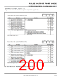
(6) RTP3
0
, RTP3 pulse output data bits (bits 4, 5 at address A416)
1
These bits are valid in pulse mode 0.
Each time when an underflow occurs in timer A8, the contents which have been written to these bits
are output from the corresponding pulse output pins (Note).
These bits are invalid in pulse mode 1.
(7) RTP3
2
, RTP3 pulse output data bits (bits 6, 7 at address A416)
3
Each time when an underflow occurs in timer A8, the contents which have been written to these bits are output
from the corresponding pulse output pins (Note).
Note: The output level at a pulse output pin is undefined in the period from when data is written to
these bits until the first occurrence of a pulse output trigger. If it is necessary to avoid this state,
perform “Processing of avoiding undefined output before starting pulse output” in Figure 9.4.2.
7905 Group User’s Manual Rev.1.0
9-20

 RENESAS [ RENESAS TECHNOLOGY CORP ]