PULSE OUTPUT PORT MODE
9.3 Block description of pulse output port 1
9.3.4 Timers A5 to A9
Timers A5 and A8 are used as control registers; each generates a pulse output trigger. When using timers
A5 and A8, be sure to use them in the timer mode. (Refer to section “7.3 Timer mode.”)
When performing the pulse width modulation, be sure to use timers A6, A7, A9 in the pulse width modulation
mode. (Refer to section “7.6 Pulse width modulation (PWM) mode.”) Note that, from pin P2
2
/TA9OUT, a
PWM pulse by timer A9 is output. When it is unnecessary to output a PWM pulse, be sure to clear bit 2
of the timer A9 mode register (address DA16) to “0.” At this time, pin P2 can be used as a programmable
2
I/O port pin.
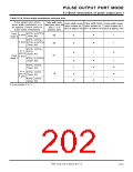
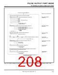
Figure 9.3.5 shows the structure of the timer A5 and A8 mode registers (pulse output port 1); Figure 9.3.6
shows the structures of the timer A6, A7, A9 mode registers (pulse output port 1 with pulse width modulation
used).
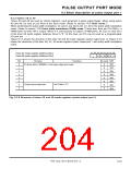
b7 b6 b5 b4 b3 b2 b1 b0
Timer A5 mode register (Address D616
Timer A8 mode register (Address D916
)
)
0 0 0 0 0 0
Bit
0
Bit name
Functions
At reset R/W
0
0
0
0
0
0
0
0
RW
RW
RW
RW
RW
RW
RW
RW
Fix these bits to “000000
2
” in the pulse output port mode.
1
2
3
4
5
See Table 7.2.3.
Count source select bits
6
7
Fig. 9.3.5 Structure of timer A5 and A8 mode registers (pulse output port 1)
7905 Group User’s Manual Rev.1.0
9-23

 RENESAS [ RENESAS TECHNOLOGY CORP ]