PULSE OUTPUT PORT MODE
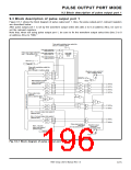
9.2 Block description of pulse output port 0
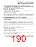
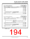
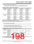
b7 b6 b5 b4 b3 b2 b1 b0
Timer A1 mode register (Address 5716
Timer A2 mode register (Address 5816
)
)
0 0 0 1 1
Bit
0
Bit name
Functions
At reset R/W
Fix these bits to “00011
2
” in the pulse output port mode.
0
0
0
0
0
0
RW
RW
RW
1
2
3
4
5
RW
RW
RW
16/8-bit PWM mode select bit
Count source select bits
0 : 16-bit pulse width modulator
1 : 8-bit pulse width modulator
6
7
See Table 7.2.3.
0
0
RW
RW
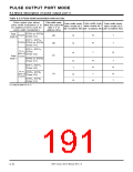
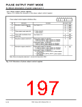
b7 b6 b5 b4 b3 b2 b1 b0
Timer A4 mode register (Address 5A16
)
0 0
1 1
Bit
0
Bit name
Fix these bits to “11
Functions
At reset R/W
2
” in the pulse output port mode.
0
0
0
RW
RW
RW
1
0 : No pulse output
Pulse output function select bit
2
(TA4OUT pin functions as a programmable I/O port
pin.)
1 : Pulse output
(TA4OUT pin functions as a PWM pulse output pin.)
Fix these bits to “00 ” in the pulse output port mode.
2
3
4
5
0
0
0
RW
RW
RW
16/8-bit PWM mode select bit
Count source select bits
0 : 16-bit pulse width modulator
1 : 8-bit pulse width modulator
6
7
See Table 7.2.3.
0
0
RW
RW
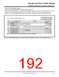
Fig. 9.2.6 Structures of timer A1, A2, A4 mode registers (pulse output port 0 with pulse width
modulation used)
7905 Group User’s Manual Rev.1.0
9-13

 RENESAS [ RENESAS TECHNOLOGY CORP ]