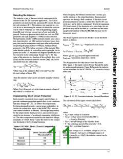
PRODUCT SPECIFICATION
RC5041
Main Control Loop
Power Good
Refer to the Block Diagram on page 1. The control loop of
the regulator contains two main sections, the analog control
block and the digital control block. The analog block con-
sists of signal conditioning amplifiers feeding into a set of
comparators which provide the inputs to the digital block.
The signal conditioning section accepts inputs from the IFB
(current feedback) and VFB (voltage feedback) pins and sets
up two controlling signal paths. The voltage control path
amplifies the VFB signal and presents the output to one of
the summing amplifier inputs. The current control path takes
the difference between the IFB and VFB pins and presents
the resulting signal to another input of the summing ampli-
fier. These two signals are then summed together with the
slope compensation input from the oscillator. This output is
then presented to a comparator, which provides the main
PWM control signal to the digital control block.
The RC5041 Power Good function is designed in accordance
with the Pentium Pro DC-DC converter specification and
provides a constant voltage monitor on the VFB pin. The
circuit compares the VFB signal to the VREF voltage and
outputs an active-low interrupt signal to the CPU should the
power supply voltage exceed ±12% of its nominal setpoint.
The Power Good flag provides no other control function to
the RC5041.
Over-Voltage Protection
The RC5041 provides a constant monitor of the output
voltage for protection against overvoltage conditions. If the
voltage at the VFB pin exceeds 20% of the selected program
voltage, an overvoltage condition will be assumed, and
the RC5041 will disable the output drive signal to the
MOSFET(s).
The additional comparators in the analog control section set
the thresholds of where the RC5041 enters its pulse skipping
mode during light loads as well as the point at which the
maximum current comparator disables the output drive sig-
nals to the external power MOSFETs.
Short Circuit Protection
A current sense methodology is implemented to disable the
output drive signal to the MOSFET(s) when an over-current
condition is detected. The voltage drop created by the output
current flowing across a sense resistor is presented to an
internal comparator. When voltage developed across the
sense resistor exceeds the comparator threshold voltage,
the RC5041 will disable the output drive signal to the
MOSFET(s).
The digital control block is designed to take the comparator
inputs along with the main clock signal from the oscillator
and provide the appropriate pulses to the HIDRV output
pin that controls the external power MOSFET. The digital
section was designed utilizing high speed Schottky transistor
logic, thus allowing the RC5041 to operate at clock speeds
as high as 1MHz.
The DC-DC converter returns to normal operation after the
fault has been removed, for either an overvoltage or a short
circuit condition.
High Current Output Drivers
Oscillator
The RC5041 contains one high current output drivers which
utilize high speed bipolar transistors arranged in a push-pull
configuration. The driver is capable of delivering 1A of cur-
rent in less than 100ns. The driver's power and ground are
separated from the overall chip power and ground for addi-
tional switching noise immunity.
The RC5041 oscillator section is implemented using a
fixed current capacitor charging configuration. An external
capacitor (CEXT) is used to preset the oscillator frequency
between 80KHz and 1MHz. This scheme allows maximum
flexibility in setting the switching frequency as well as
choosing external components.
Internal Voltage Reference
In general, a lower operating frequency will increase the
peak ripple current flowing in the output inductor, and thus
require the use of a larger inductor value. Operation at lower
frequencies also increases the amount of energy storage that
must be provided by the bulk output capacitors during load
transients due to the slower loop response of the controller.
The reference included in the RC5041 is a 1.24V precision
band-gap voltage reference. The internal resistors are pre-
cisely trimmed to provide a near zero temperature coefficient
(TC). Added to the reference input is the resulting output
from an integrated 4-bit DAC. The DAC is provided in
accordance with the Pentium Pro specification guideline,
which requires the DC-DC converter output to be directly
programmable via a 4-bit voltage identification (VID) code.
This code will scale the reference voltage from 2.0V (no
CPU) to 3.5V in 100mV increments. For guaranteed stable
operation under all loading conditions, a 10KΩ pull-up
resistor and 0.1µF of decoupling capacitance should be
connected to the VREF pin.
The user should note that the efficiency losses due to switch-
ing are relatively fixed per switching cycle. Therefore, as the
switching frequency is increased, so is the contribution
toward efficiency due to switching losses.
Careful analysis of the RC5041 DC-DC controller has
resulted in an optimal operating frequency of 300KHz,
which allows the use of smaller inductive and capacitive
components while maximizing peak efficiency under all
operating conditions.
7

 RAYTHEON [ RAYTHEON COMPANY ]