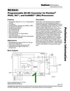
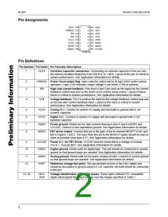
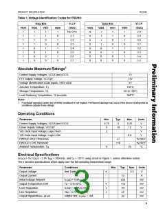
RC5041
PRODUCT SPECIFICATION
Electrical Specifications (continued)
(V
CCA
= 5V, V
OUT
= 2.8V, f = 300 KHz, and T = +25°C using circuit in Figure 1, unless otherwise noted)
osc A
The • denotes specifications which apply over the full operating temperature range.
Parameter
Conditions
Min.
Typ. Max. Units
Output Voltage Regulation
Steady State1
V
I
= 2.8V, I
LOAD
= 0 to 10A
= 0.8 to 9.5A, 30A/µS
•
•
2.74
2.70
2.80
2.80
2.90
2.90
V
V
OUT
LOAD
Transient2
Efficiency
I
= 10A, V
OUT
= 2.8V
•
80
85
50
%
ns
LOAD
Output Driver Rise and Fall Time
Turn-on Response Time
Oscillator Range
See Figure 2
I
= 0A to 10A
10
ms
KHz
KHz
%
LOAD
80
90
300
300
95
1000
Oscillator Frequency
Maximum Duty Cycle
Notes:
C
EXT
= 100 pF
1. Steady State Voltage Regulation includes Initial Voltage Setpoint, DC load regulation, outut ripple/noise and temperature drift.
2. These specifications assume a minimum of 20, 1µF ceramic capacitors are placed directly next to the CPU in order to provide
adequate high-speed decoupling. For motherboard applications, the PCB layout must exhibit no more than 0.5mΩ parasitic
resistance and 1nH parasitic inductance between the converter output and the CPU.
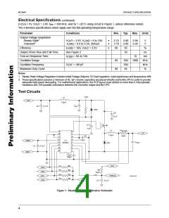
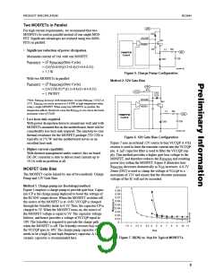
Test Circuits
+12V
L2
VCC
2.5µH
C
C4
0.1µF
IN
DS2
C8
0.1
F
µ
C12
M1
1µF
R
L1
1.0µH
9
10
11
12
8
7
6
5
4
3
2
1
SENSE
VO
6mΩ
C6
1.0µF
U1
RC5041
VREF
GND
C
13
14
15
16
OUT
DS1
C7
0.1µF
C
EXT
100pF
R1
10K
10K
VCC
VID3
VID2
R2
R6
10KΩ
R3
R4
10K
10K
PWRGD
VID1
VID0
65-5041-03
VCC
C11
0.1µF
Figure 1. Standard Test or Application Schematic
4

 RAYTHEON [ RAYTHEON COMPANY ]