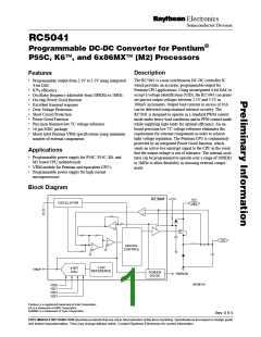
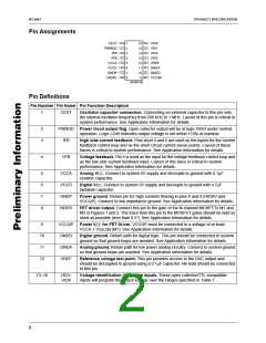
PRODUCT SPECIFICATION
RC5041
Table 1. Voltage Identification Codes for P55/K6
Data Bits
VID2 VID1
V
P
Data Bits
VID2 VID1
V
P
CC
CC
VID3
VID0
(VDC)
No CPU
2.1
VID3
VID0
(VDC)
2.8
1
1
1
1
1
1
1
1
1
1
1
1
0
0
0
0
1
1
0
0
1
1
0
0
1
0
1
0
1
0
1
0
0
0
0
0
0
0
0
0
1
1
1
1
0
0
0
0
1
1
0
0
1
1
0
0
1
0
1
0
1
0
1
0
2.9
2.2
3.0
2.3
3.1
2.4
3.2
2.5
3.3
2.6
3.4
2.7
3.5
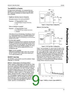
Absolute Maximum Ratings1
Control Supply Voltages, VCCA and VCCD
FET Supply Voltage, VCCQP
7V
13V
7V
Voltage Identification Code Inputs, VID3-VID0
Junction Temperature, T
150˚C
J
Storage Temperature, T
-65 to 150˚C
300˚C
S
Lead Soldering Temperature, 10 seconds
Notes:
1. Functional operation under any of these conditions is not implied. Permanent damage may occur if the device is subjected to
conditions outside these ratings.
Operating Conditions
Parameter
Min.
4.75
9
Typ.
5
Max.
5.25
12
Units
Control Supply Voltages, VCCA and VCCD
Driver Supply Voltage, VCCQP
VID Code Input Voltage, Logic HIGH
VID Code Input Voltage, Logic LOW
PWRGD HIGH Threshold
V
10
V
V
2
0.8
70
V
±7
%VREF
%VREF
°C
PWRGD LOW Threshold
±10
Ambient Temperature, T
0
A
Electrical Specifications
(V
CCA
= 5V, V
OUT
= 2.8V, f = 300 KHz, and T = +25°C using circuit in Figure 1, unless otherwise noted)
osc A
The • denotes specifications which apply over the full operating temperature range.
Parameter
Conditions
Min.
Typ. Max. Units
Output Voltage
See Table 1
•
3.5
V
Output Current
13
±20
+10
-20
±2
A
Initial Voltage Setpoint
Output Temperature Drift
Load Regulation
I
= 0.8A
mV
mV
mV
mV
mV
LOAD
T = 0 to 60°C
•
•
•
A
I
= 0.8A to 10A
LOAD
Line Regulation
V
= 4.75V to 5.25V
IN
Output Ripple/Noise, pk-pk
20MHz BW, I
LOAD
= 10A
20
3

 RAYTHEON [ RAYTHEON COMPANY ]