PRODUCT SPECIFICATION
RC5041
Two MOSFETs in Parallel
+5V
For high current requirements, we recommend that two
MOSFETs be used in parallel instead of one single MOS-
FET. Significant advantages are realized using two MOS-
FETs in parallel:
DS2
CP
VCCQP
HIDRV
M
L1
RS
• Significant reduction of power dissipation.
VO
PWM/PFM
Control
Maximum current of 14A with one MOSFET:
CB
DS1
P
= (I2 R
)(Duty Cycle)
DS(ON)
MOSFET
= (14)2(0.050*)(3.3+0.4)/(5+0.4-0.35)
65-5041-07
= 7.2 W
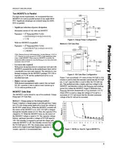
Figure 5. Charge Pump Configuration
Method 2. 12V Gate Bias
With two MOSFETs in parallel:
= (I2 R
)(Duty Cycle)
P
MOSFET
DS(ON)
+5V
= (14/2)2(0.037*)(3.3+0.4)/(5+0.4-0.35)
47Ω
+12V
DS2
6.2V
= 1.3W/FET
VCCQP
HIDRV
*Note: R
25°C. R
DS(on)
increases with temperature. Assume R
= 0.025 at
can easily increase to 0.050W at high temperature when
DS(on)
DS(on)
M1
using a single MOSFET. When using two MOSFETs in parallel, the
temperature effects should not cause the R
maximum value of 37mW.
to rise above the listed
DS(on)
L1
RS
VO
PWM/PFM
Control
• Less heat sink required.
CB
DS1
With power dissipation down to around one watt and with
MOSFETs mounted flat on the motherboard, there will be
considerably less heat sink required. The junction-to-case
thermal resistance for the MOSFET package (TO-220) is
typically at 2°C/W and the motherboard serves as an
excellent heat sink.
65-5041-08
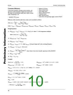
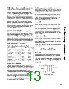
Figure 6. 12V Gate Bias Configuration
Figure 7 uses an external 12V source to bias VCCQP. A 47Ω
resistor is used to limit the transient current into the VCCQP
pin. A 1µF capacitor filter is used to filter the VCCQP sup-
ply. This method provides a higher gate bias voltage to the
• Higher current capability.
With thermal management under control, this on-board
DC-DC converter is able to deliver load currents up to
14.5A with no problem at all.
MOSFET, and therefore reduces the R
SD(ON)
and resulting
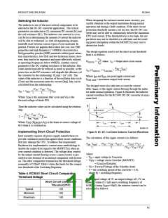
power loss within the MOSFET. Figure 8 illustrates how
R
decreases dramatically as V increases. A 6.2V
DS(ON)
GS
MOSFET Gate Bias
Zener (DS2) is used to clamp the voltage at V
to a
CCQP
The MOSFET can be biased by one of two methods: Charge
Pump and 12V Gate Bias.
maximum of 12V and ensure that the absolute maximum
voltage of the IC will not be exceeded.
Method 1. Charge pump (or Bootstrap) method
0.1
0.09
0.08
0.07
0.06
0.05
0.04
0.03
0.02
0.01
0
Figure 5 employs a charge pump to provide gate bias. Capac-
itor CP is the charge pump deployed to boost the voltage of
the RC5041 output driver. When the MOSFET switches off,
the source of the MOSFET is at -0.6V. VCCQP is charged
through the Schottky diode to 4.5V. Thus, the capacitor CP is
charged to 5V. When the MOSFET turns on, the source of
the MOSFET voltage is equal to 5V. The capacitor voltage
follows, and hence provides a voltage at VCCQP equal to
10V. The Schottky is required to provide the charge path
when the MOSFET is off. The Schottky reverses bias when
the VCCQP goes to 10V. The charge pump capacitor, CP,
needs to be a high Q and high frequency capacitor. A 1µF
ceramic capacitor is recommended here.
1.5 2 2.5 3 3.5 4
5
6
7
8
9
10 11
V
GS
Figure 7. R(DS) vs. V
GS
for Typical MOSFETs
9

 RAYTHEON [ RAYTHEON COMPANY ]