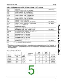
RC5041
PRODUCT SPECIFICATION
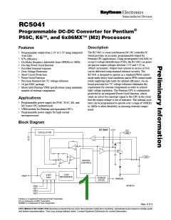
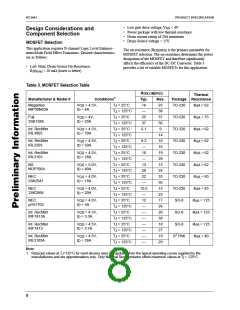
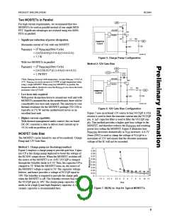
Pin Assignments
CEXT
PWRGD
IFB
1
2
3
4
5
6
7
8
16
15
14
13
12
11
10
VID0
VID1
VID2
VFB
VID3
VCCA
VCCD
GNDP
HIDRV
VREF
GNDA
GNDD
VCCQP
9
65-5041-02
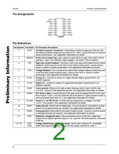
Pin Definitions
Pin Number Pin Name Pin Function Description
1
CEXT
Oscillator capacitor connection. Connecting an external capacitor to this pin sets
the internal oscillator frequency from 200 KHz to 1 MHz. Layout of this pin is critical to
system performance. See Application Information for details.
2
3
PWRGD Power Good output flag. Open collector output will be at logic HIGH under normal
operation. Logic LOW indicates output voltage is not within ±10% of nominal.
IFB
High side current feedback. Pins short 4 and 5 are used as the inputs for the current
feedback control loop and as the short circuit current sense points. Layout of these
traces is critical to system performance. See Application Information for details.
4
VFB
Voltage feedback. Pin 5 is used as the input for the voltage feedback control loop and
as the low side current feedback input. Layout of this trace is critical to system
performance. See Application Information for details.
5
6
7
8
VCCA
VCCD
GNDP
HIDRV
Analog V . Connect to system 5V supply and decouple to ground with 0.1µF
ceramic capacitor.
CC
Digital V . Connect to system 5V supply and decouple to ground with 4.7µF
CC
tantalum capacitor.
Power ground. Return pin for high currents flowing in pins 8 and 9 (HIDRV and
VCCQP). Connect to low impedance ground. See Application Information for details.
FET driver output. Connect this pin to the gate of the N-channel MOSFETs M1 and
M2 in Figures 1 and 2. The trace from this pin to the MOSFET gates should be kept as
short as possible (less than 0.5"). See Application Information for details.
9
VCCQP
GNDD
GNDA
VREF
Power V
CC
VCCA + V
GS,ON
for FET Driver. VCCQP must be connected to a voltage of at least
(M1). See Application Information for details.
10
11
12
Digital ground. Return path for digital logic. This pin should be connected to system
ground so that ground loops are avoided. See Application Information for details.
Analog ground. Return path for low power analog circuitry. Connect to system ground
so that ground loops are avoided. See Application Information for details.
Reference voltage test point. This pin provides access to the DAC output and
should be decoupled to ground using a 0.1µF capacitor. No load should be connected
to this pin.
13–16
VID3–
VID0
Voltage identification (VID) code inputs. These open collector/TTL compatible
inputs will program the output voltage over the ranges specified in Table 1.
2

 RAYTHEON [ RAYTHEON COMPANY ]