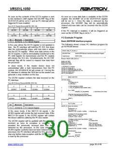
VRS51L1050
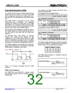
PWM Data Registers
Notes on PWM Use
The following tables describe the PWM0 and PWM1
data registers. The PWMDx bits hold the contents of
the PWM data register and determine the duty cycle of
the PWM output waveforms.
To activate the PWM modules follow the procedure
below:
1. Set the PWM data register
2. Set the PWM operating frequency and PWM
resolution by setting the PWMCTRLx register
3. Activate the PWM output by setting the
corresponding PWMxE bit of the PWMCTRLx
register
TABLE 41: PWM0 DATA REGISTER (PWMD0) – SFR B3H
7
6
5
4
PWMD0.7
PWMD0.6
PWMD0.5
PWMD0.4
3
2
1
0
The selected PWM module operation will begin if:
PWMD0.4
PWMD0.3
PWMD0.2
PWMD0.1
o
The Port 1 I/O pins associated with the PWM
outputs are configured to output a logic 0.
Bit Mnemonic
Description
PWM0 Data Register
7
PWMD0[7:0]
o
The PWM module is enabled before the PWM
data is configured. The PWM output will
momentarily go to 0 for a duration equal to the
time the PWM was enabled and data will be
written into the I2CPWMDx register.
TABLE 42: PWM1 DATA REGISTER (PWMD1) – SFR B4H
7
6
5
4
PWMD1.7
PWMD1.6
PWMD1.5
PWMD1.4
3
2
1
0
PWMD1.4
PWMD1.3
PWMD1.2
PWMD1.1
o
If the I2CPWMDx register is set to FFh, the
PWM will output 1 the entire time, but the
output will go low momentarily (1.5 us) on
each PWM cycle.
Bit Mnemonic
Description
PWM1 Data Register
7
PWMD1[7:0]
The PWM modules are not data buffered. As such,
updating the PWM data register will have an immediate
impact on the PWM output.
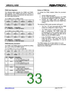
PWM Modules Activation
The PWM1 and PWM0 outputs are activated by setting
bits 3 and 2 of the I2CPWME register.
TABLE 43: I2CPWME CONFIGURATION REGISTER (I2CPWME, $9B)
7
6
5
-
4
-
SDAE
SCLE
3
2
1
-
0
-
PWM1E
PWM0E
Bit
7
Mnemonic
SDAE
Description
I²C SDA Enable
0: P1.7I/O is dedicated to I²C SDA
1: P1.7 I/O operate as regular I/O
I²C SCL Enable
6
SCLE
0: P1.6I/O is dedicated to I²C SCL
1: P1.6 I/O operate as regular I/O
5
4
3
-
-
PWM1E
PWM1 Enable Register
0 = PWM1 module is deactivated
1 = PWM1 module is activated on P1.3
2
PWM0E
PWM1 Enable Register
0 = PWM0 module is deactivated
1 = PWM0 module is activated on P1.3
1
0
-
-
______________________________________________________________________________________________
www.ramtron.com page 33 of 49

 RAMTRON [ RAMTRON INTERNATIONAL CORPORATION ]