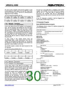
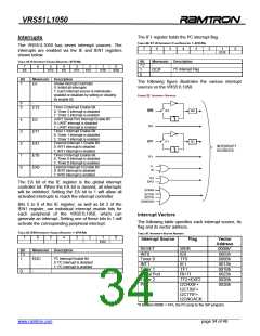
VRS51L1050
The following two tables describe the PWM control
registers’ bit assignment:
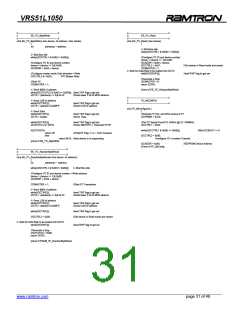
Pulse Width Modulation (PWM)
TABLE 39: PWM0 CONTROL REGISTER PWMCTRL0–SFR D3H
The VRS51L1050 provides two PWM outputs that are
shared with the P1.2 and P1.3 I/O pins. Each PWM
can be configured to operate with a resolution of 8 or 5
bits, with the 5-bit mode allowing a faster PWM output
rate.
7
6
5
-
4
3
2
1
0
PWMCK1
PWMCK0
5BITE
Bit
[7:3]
2
Mnemonic
Description
-
5 Bit PWM operation enable
0 = PWM0 resolution is 8 bit
1 = PWM0 resolution is 5 bit
-
Each PWM module is composed of a free running
timer/counter and a comparator. The comparator
compares the PWM free running timer to the PWM
data register. The comparator output will remain high
as long as the value of the free running timer is lower
than the value present in the PWMDx register.
5BITE
1
0
PWMCK1
PWMCK0
Clock Frequency Divider Bit 1 for PWM0
Clock Frequency Divider Bit 0 for PWM0
TABLE 40: PWM1 CONTROL REGISTER (PWMCTRL1–SFR D4H)
7
6
5
-
4
3
2
1
0
Once the value of the PWM timer equals the value in
the PWMDx register, the PWM output will be set to 0
and will remain in that state until the PWM timer
overflows.
PWMCK1
PWMCK0
5BITE
Bit
[7:3]
2
Mnemonic
Description
-
5 Bit PWM operation enable
0 = PWM1 resolution is 8 bit
1 = PWM1 resolution is 5 bit
-
5BITE
The maximum timer value before an automatic
overflow and restart occurs depends on the
configuration of the PWM module. When the PWM
module is configured to operate at 8 bits, the overflow
will occur at FFh. When the PWM module is configured
to operate in 5-bit mode, the overflow will occur at 1Fh.
1
0
PWMCK1
PWMCK0
Clock Frequency Divider Bit 1 for PWM1
Clock Frequency Divider Bit 0 for PWM1
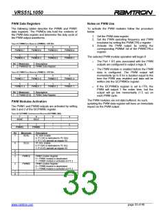
The following table describes the relationship between
the values of PWMCK1, PWMCK0 and the numerical
divider values of the corresponding frequencies.
The following diagram demonstrates the relationship
between the PWM output vs. the PWM timer, when the
PWM module is configured in 8-bit mode.
PWMCK1 PWMCKO Divider
0
0
1
1
0
1
0
1
4
8
16
32
FIGURE 21: PWM OUTPUT VS. PWM TIMER VALUE
Cycle 1
Cycle 2
Port 1.2 /
P1.3
The PWM output frequency is calculated using the
following two formulas:
PWM
FFh 00h
FFh 00h
I2CPWMDx
I2CPWMDx
Enable
8-bit PWM Rate =
Fosc
[256x 2(PWMCK[1:0] +2)
]
There is no interrupt associated with the PWM
modules.
PWM Control Registers
The PWMCTRL0 and PWMCTRL1 registers control
the operating frequency and the resolution of each
PWM module.
5-bit PWM Rate =
Fosc
[32x 2(PWMCK[1:0] +2)
]
______________________________________________________________________________________________
www.ramtron.com page 32 of 49

 RAMTRON [ RAMTRON INTERNATIONAL CORPORATION ]