VRS51L1050
As soon as the contents of the I2CTX register is sent
to the interface’s shift register the I2CTXIF flag of the
I2CSTATUS will be set to 1 and an I²C interrupt will be
triggered if it was enabled.
As soon as a new data byte is available in the I2CRX
register, the I2CRXIF bit of the I2CSTATUS register
will be set to 1. Once the data is retrieved by the
processor, the I2CRXIF flag will be automatically
cleared and new data can be received into the I2CRX
register.
TABLE 37: I²C TRANSMIT REGISTER (I2CTX) - SFR –C4H
7
6
5
4
I2CTX7
I2CTX6
I2CTX5
I2CTX4
If the I²C interrupt is enabled, it will be triggered as
soon as the I2CRXIF flag is set to 1.
3
2
1
0
I2CTX3
I2CTX2
I2CTX1
I2CTX0
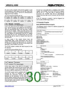
I²C Example Program
Bit
7:0
Mnemonic
I2CTX[7:0]
Description
I²C Transmit Register
Basic EEPROM interface program
The following shows a basic I²C interface program for
an EEPROM device
In the case where the I2CTX register is not updated in
time, the I²C interface will hold the I²C SCL line down
after the acknowledge phase until new data is written
into the I2CTX register. When new data arrives in the
I2CTX register, it will be immediately transferred to the
I²C shift register for transmission and the I²C module
will release the SCL line. Simultaneously, the I2CTXIF
interrupt flag will be raised to request new data from
the processor.
//-----------------------------------------------------------------------------------------------------------------//
// VRS51L1050_I²C_24xx64.c //
//-----------------------------------------------------------------------------------------------------------------//
// DESCRIPTION:
//
24xx64 EERPOM basic interface Demonstration Program.
// Target Device:
VRS51L1050
//-----------------------------------------------------------------------------------------------------------------//
#include <VRS51L1050_SDCC.h>
#define OK 0x01;
#define BUG 0x00;
#define BUSY 0x00;
In slave mode, if the master device does not
acknowledge after a byte transmission from the I²C
module, the I2CRXACK bit will remain at 1 forcing the
I²C interface to release the SDA line so the master can
generate a stop condition on the bus.
//--EEPROM I²C Functions
char EE_I²C_Busy( char );
char EE_I²C_ByteWrite( char, int, char);
char EE_I²C_RandomByteRead( char, int);
char EE_I²C_Read( char );
void I²C_MConfig(void );
//-----------------------------------------------------------------------------------------------------------------//
//
MAIN FUNCTION
The I2CRX register contains the data received on the
I²C interface.
//-----------------------------------------------------------------------------------------------------------------//
void main (void) {
char x;
//--Configure the I²C
I²C_MConfig( );
TABLE 38: I²C RECEIVE REGISTER (I2CRX) - SFR –C5H
//--Write Data Byto to FRAM
x = EE_I²C_ByteWrite( 0x00, 0x0302, 0x0F);
7
6
5
4
//
I2CRX7
I2CRX6
I2CRX5
I2CRX4
//
//
if(x == 0x00)
while(!EE_I²C_Busy(0x00));
//--wait Device to be ready
//Read the Data byte from the EEPROM
x = EE_I²C_RandomByteRead( 0x00, 0x0302);
3
2
1
0
while(1);
}// End of main
I2CRX3
I2CRX2
I2CRX1
I2CRX0
//---------------------------------------------------//
//;
EE_I²C_Busy
//---------------------------------------------------//
char EE_I²C_Busy( char device)
Bit
Mnemonic
Description
I²C Transmit Register
{
7:0
I2CRX[7:0]
I2CNOACKF = 0;
I2CTXACK = 0;
In the slave mode, if the MATCH bit equals 1, the
I2CRX register will contain the last received data. If the
MATCH bit equals 0, the I2CRX register will contain
the device address called by the I²C bus master.
while((I2CCTRL1 & 0x08) != 0x00){};
//--Wait Bus idle
//Configure I²C ID and device number
device = (device << 2)& 0x0E;
I2CADDR = 0xA0 + device;
//Configure master mode Data direction = Write
I2CCTRL2 &= 0xFE;
//Start I²C
I2CMASTER = 1;
while((I2CTXIF) == 0x00){};
I2CMASTER = 0;
//I²C Master Write
The I2CRX register will be updated with the new data
received as soon its reception is complete and
provided the previously received data has been
retrieved by the processor. In the case where the
I2CRX register contents have not been retrieved by the
processor, the I²C interface will pull the SCL line low to
stop any further data reception until the I2CRX register
is read by the processor.
//Start Transaction
//wait TXIF flag to get set
//Generate a stop condition
while((I2CCTRL1 & 0x08) != 0x00){};
//--Wait Bus idle
if(I2CNOACKF)
return BUSY
else
return OK;
}//end of EE_I²C_Busy
______________________________________________________________________________________________
www.ramtron.com page 30 of 49

 RAMTRON [ RAMTRON INTERNATIONAL CORPORATION ]