VRS51C1000
TABLE 31: SERIAL PORT MODES OF OPERATION
UART Transmission in Mode 0
SM0
SM1
0
1
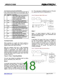
Mode
Description
Baud Rate
Fosc/12
Variable
Fosc/64 or
0
0
1
0
1
2
Shift Register
8-bit UART
9-bit UART
Any instruction that uses SBUF as a destination
register may initiate a transmission. The “write to
SBUF” signal also loads a 1 into the 9th position of the
transmit shift register and informs the TX control block
to begin a transmission. The internal timing is such that
one full machine cycle will elapse between a write to
SBUF instruction and the activation of SEND.
0
Fosc/32
1
1
3
9-bit UART
Variable
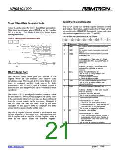
UART Operating Modes
The VRS51C1000’s serial port can operate in four
different Modes. In all four Modes, a transmission is
initiated by an instruction that uses the SBUF register
as a destination register. In Mode 0, reception is
initiated by setting RI to 0 and REN to 1. An incoming
start bit initiates reception in the other modes, provided
that REN is set to 1. The following paragraphs
describe these four Modes.
The SEND signal enables the output of the shift
register to the alternate output function line of P3.0 and
enables SHIFT CLOCK to the alternate output function
line of P3.1.
At every machine cycle in which SEND is active, the
contents of the transmit shift register are shifted to the
right by one position.
UART Operation in Mode 0
Zeros come in from the left as data bits shift out to the
right. The TX control block sends its final shift and de-
activates SEND while setting T1 after one condition is
fulfilled. When the MSB of the data byte is at the
output position of the shift register; the 1 that was
initially loaded into the 9th position is just to the left of
the MSB; and all positions to the left of that contain
zeros. Once these conditions are met, the de-
activation of SEND and the setting of T1 occurs at T1
of the 10th machine cycle after the “write to SBUF”
pulse.
In this Mode, the serial data exits and enters through
the RXD pin. TXD is used to output the shift clock. The
signal is composed of 8 data bits starting with the LSB.
The baud rate in this mode is 1/12 the oscillator
frequency.
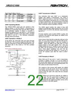
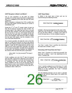
FIGURE 16: SERIAL PORT MODE 0 BLOCK DIAGRAM
Internal Bus
1
Write to
SBUF
Q
S
D
SBUF
RXD P3.0
Shift
CLK
UART Reception in Mode 0
ZERO DETECTOR
Shift
Clock
TXD P3.1
Shift
Start
When REN and R1 are set to 1 and 0, respectively,
reception is initiated. The bits 11111110 are written to
the receive shift register at the end of the next machine
cycle by the RX control unit. In the following phase, the
RX control unit will activate RECEIVE.
TX Control Unit
TX Clock
Send
Fosc/12
TI
Serial Port
Interrupt
RI
RX Clock
Receive
RX Control Unit
RI
REN
Start Shift
1
1
1
1
1
1
1
0
The contents of the receive shift register are shifted
one position to the left at the end of every machine
cycle during which RECEIVE is active. The value that
comes in from the right is the value that was sampled
at the P3.0 pin.
RXD P3.0
Input Function
RXD P3.0
Shift Register
READ SBUF
SBUF
Internal Bus
1’s are shifted out to the left as data bits are shifted in
from the right. The RX control block is flagged to do
one last shift and load SBUF when the 0 that was
initially loaded into the rightmost position arrives at the
leftmost position in the shift register.
______________________________________________________________________________________________
www.ramtron.com page 22 of 48

 RAMTRON [ RAMTRON INTERNATIONAL CORPORATION ]