VRS51C1000
UART Operation in Mode 3
UART in Mode 2 and 3: Additional Information
In Mode 3, 11 bits are transmitted (through TXD) or
received (through RXD). The transactions are
composed of: a Start bit (Low), 8 data bits (LSB first), a
programmable 9th data bit, and one Stop bit (High).
As mentioned previously, for an operation in Modes 2
and 3, 11 bits are transmitted (through TXD) or
received (through RXD). The signal comprises: a
logical low Start bit, 8 data bits (LSB first), a
programmable 9th data bit, and one logical high Stop
bit.
On transmit, (TB8 in SCON) can be assigned the value
of 0 or 1. On receive; the 9th data bit goes into RB8 in
SCON. The baud rate is programmable to either 1/32
or 1/64 the oscillator frequency in Mode 2. Mode 3 may
have a variable baud rate generated from either Timer
1 or Timer 2 depending on the states of TCLK and
RCLK.
Mode 3 is identical to Mode 2 in all respects but one:
the baud rate. Either Timer 1 or Timer 2 generates the
baud rate in Mode 3.
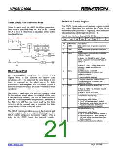
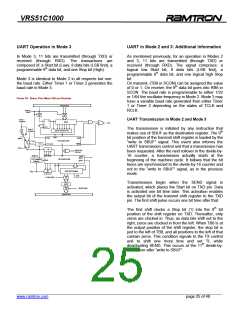
FIGURE 19: SERIAL PORT MODE 3 BLOCK DIAGRAM
Internal Bus
1
Write to
SBUF
Timer 1
Overflow
UART Transmission in Mode 2 and Mode 3
Q
S
D
SBUF
TXD
CLK
Timer 2
Overflow
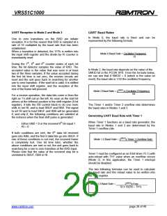
The transmission is initiated by any instruction that
makes use of SBUF as the destination register. The 9th
bit position of the transmit shift register is loaded by the
“write to SBUF” signal. This event also informs the
UART transmission control unit that a transmission has
been requested. After the next rollover in the divide-by-
16 counter, a transmission actually starts at the
beginning of the machine cycle. It follows that the bit
times are synchronized to the divide-by-16 counter and
not to the “write to SBUF” signal, as in the previous
mode.
ZERO DETECTOR
÷2
0
1
Shift
Start
Data
SMOD
0
0
1
TX Control Unit
TCLK
TX Clock
÷16
Send
÷16
TI
1
RCLK
Serial Port
Interrupt
RI
SAMPLE
RX Clock
Start
Load
SBUF
RX Control Unit
1-0 Transition
Detector
SHIFT
Bit
Detector
9-Bit Shift Register
Shift
RXD
LOAD SBUF
Transmissions begin when the SEND signal is
activated, which places the Start bit on TXD pin. Data
is activated one bit time later. This activation enables
the output bit of the transmit shift register to the TXD
pin. The first shift pulse occurs one bit time after that.
SBUF
READ SBUF
Internal Bus
The first shift clocks a Stop bit (1) into the 9th bit
position of the shift register on TXD. Thereafter, only
zeros are clocked in. Thus, as data bits shift out to the
right, zeros are clocked in from the left. When TB8 is at
the output position of the shift register, the stop bit is
just to the left of TB8, and all positions to the left of that
contain zeros. This condition signals to the TX control
unit to shift one more time and set TI, while
deactivating SEND. This occurs at the 11th divide-by-
16 rollover after “write to SBUF”.
______________________________________________________________________________________________
www.ramtron.com page 25 of 48

 RAMTRON [ RAMTRON INTERNATIONAL CORPORATION ]