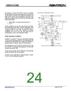
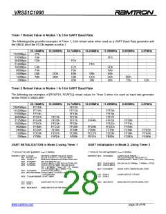
VRS51C1000
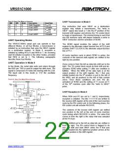
FIGURE 18: SERIAL PORT MODE 2 BLOCK DIAGRAM
bit register), it causes the UART’s receive controller
block to perform one last shift operation: to set RI and
to load SBUF and RB8. The signal to load SBUF and
RB8, and to set RI, will be generated if, and only if, the
following conditions are met at the time the final shift
pulse is generated:
Internal Bus
1
Write to
SBUF
Q
S
D
SBUF
Fosc/2
÷2
TXD
o
o
Either SM2 = 0 or the received stop bit = 1
RI = 0
CLK
ZERO DETECTOR
0
1
If both conditions are met, the stop bit goes into RB8,
the 8 data bits go into SBUF, and RI is activated. If one
of these conditions is not met, the received frame is
completely lost. At this time, whether the above
conditions are met or not, the unit goes back to
searching for a one to zero transition in RXD.
Shift
Data
Stop
Start
SMOD
TX Control Unit
TX Clock
Send
÷16
TI
÷16
Serial Port
Interrupt
Sample
RI
RX Clock
Control
Load
SBUF
RX Control Unit
1-0 Transition
Detector
Start
SHIFT
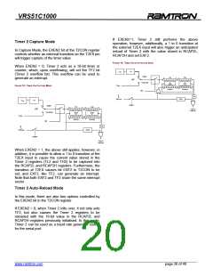
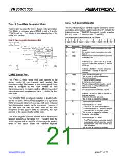
UART Operation in Mode 2
Bit
Detector
9-Bit Shift Register
Shift
RXD
In Mode 2 a total of 11 bits are transmitted (through
TXD) or received (through RXD). The transactions are
composed of: a Start bit (Low), 8 data bits (LSB first), a
programmable 9th data bit, and one Stop bit (High).
LOAD SBUF
SBUF
READ SBUF
For transmission, the 9th data bit comes from the TB8
bit of SCON. For example, the parity bit P in the PSW
could be moved into TB8.
Internal Bus
In the case of receive, the 9th data bit is automatically
written into RB8 of the SCON register.
In Mode 2, the baud rate is programmable to either
1/32 or 1/64 the oscillator frequency.
______________________________________________________________________________________________
www.ramtron.com page 24 of 48

 RAMTRON [ RAMTRON INTERNATIONAL CORPORATION ]